First integration of Ni barrier layer for enhanced threshold switching characteristics in Ag/HfO2-based TS device

IF 8.1 2区 材料科学 Q1 MATERIALS SCIENCE, MULTIDISCIPLINARY
Daeyoung Chu, Sanghyun Kang, Gwon Kim, Juho Sung, Jaehyuk Lim, Yejoo Choi, Donghwan Han, Changhwan Shin
{"title":"First integration of Ni barrier layer for enhanced threshold switching characteristics in Ag/HfO2-based TS device","authors":"Daeyoung Chu, Sanghyun Kang, Gwon Kim, Juho Sung, Jaehyuk Lim, Yejoo Choi, Donghwan Han, Changhwan Shin","doi":"10.1016/j.mtadv.2024.100492","DOIUrl":null,"url":null,"abstract":"Utilizing Ag/HfO with nickel (Ni) as a barrier layer, a novel threshold switching (TS) device is devised to overcome challenges such as low reliability, high threshold voltage, and high leakage current. Compared against an Ag/Ti/HfO-based TS device, the Ag/Ni/HfO-based TS device exhibits improved electrical characteristics: yield enhancement from 31.7 % to 40.0 %, enhanced endurance from ∼10 cycles to ∼300 cycles, and suppression in off-state current (I) from 1.2 × 10 A to 5.2 × 10 A under a high compliance current (e.g., 10 A). The results obtained through transmission electron microscopy (TEM), energy-dispersive X-ray spectroscopy (EDS), and atomic force microscopy (AFM) support the evidence of those accomplishments. Reducing the effective area of the TS device improves control over erratically generated filaments and the electric field within the switching layer, resulting in enhanced performance such as a reduced threshold voltage (V ∼0.35 V), minimized V variability (∼0.01 V), decreased a threshold current (I, i.e., the leakage current in the off-state before activation, ∼5.2 × 10 A), and maximum conductance (∼5.0 × 10 S) of low-resistance state. These findings suggest that the optimized Ag/Ni/HfO-based TS device can serve as a practical solution for low-power applications.","PeriodicalId":48495,"journal":{"name":"Materials Today Advances","volume":"72 1","pages":""},"PeriodicalIF":8.1000,"publicationDate":"2024-05-03","publicationTypes":"Journal Article","fieldsOfStudy":null,"isOpenAccess":false,"openAccessPdf":"","citationCount":"0","resultStr":null,"platform":"Semanticscholar","paperid":null,"PeriodicalName":"Materials Today Advances","FirstCategoryId":"88","ListUrlMain":"https://doi.org/10.1016/j.mtadv.2024.100492","RegionNum":2,"RegionCategory":"材料科学","ArticlePicture":[],"TitleCN":null,"AbstractTextCN":null,"PMCID":null,"EPubDate":"","PubModel":"","JCR":"Q1","JCRName":"MATERIALS SCIENCE, MULTIDISCIPLINARY","Score":null,"Total":0}
引用次数: 0

Abstract

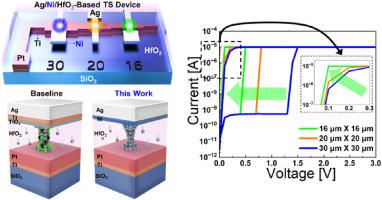
Utilizing Ag/HfO with nickel (Ni) as a barrier layer, a novel threshold switching (TS) device is devised to overcome challenges such as low reliability, high threshold voltage, and high leakage current. Compared against an Ag/Ti/HfO-based TS device, the Ag/Ni/HfO-based TS device exhibits improved electrical characteristics: yield enhancement from 31.7 % to 40.0 %, enhanced endurance from ∼10 cycles to ∼300 cycles, and suppression in off-state current (I) from 1.2 × 10 A to 5.2 × 10 A under a high compliance current (e.g., 10 A). The results obtained through transmission electron microscopy (TEM), energy-dispersive X-ray spectroscopy (EDS), and atomic force microscopy (AFM) support the evidence of those accomplishments. Reducing the effective area of the TS device improves control over erratically generated filaments and the electric field within the switching layer, resulting in enhanced performance such as a reduced threshold voltage (V ∼0.35 V), minimized V variability (∼0.01 V), decreased a threshold current (I, i.e., the leakage current in the off-state before activation, ∼5.2 × 10 A), and maximum conductance (∼5.0 × 10 S) of low-resistance state. These findings suggest that the optimized Ag/Ni/HfO-based TS device can serve as a practical solution for low-power applications.
Abstract Image

在基于 Ag/HfO2 的 TS 器件中首次集成镍阻挡层以增强阈值开关特性
利用镍(Ni)作为阻挡层的 Ag/HfO 设计了一种新型阈值开关(TS)器件,以克服低可靠性、高阈值电压和高漏电流等挑战。与基于 Ag/Ti/HfO 的 TS 器件相比,基于 Ag/Ni/HfO 的 TS 器件具有更好的电气特性:良率从 31.7% 提高到 40.0%;耐久性从 10 次循环提高到 300 次循环;在高顺从电流(如 10 A)条件下,离态电流 (I) 从 1.2 × 10 A 抑制到 5.2 × 10 A。通过透射电子显微镜(TEM)、能量色散 X 射线光谱(EDS)和原子力显微镜(AFM)获得的结果也证明了这些成就。减小 TS 器件的有效面积可改善对开关层内不规则产生的灯丝和电场的控制,从而提高性能,如降低阈值电压(V ∼ 0.35 V)、最大限度地减少 V 变化(∼ 0.01 V)、减小阈值电流(I,即关断状态下的漏电流)、5.2 × 10 A)和低电阻状态的最大电导(∼5.0 × 10 S)。这些研究结果表明,经过优化的 Ag/Ni/HfO 基 TS 器件可以作为低功耗应用的实用解决方案。
本文章由计算机程序翻译,如有差异,请以英文原文为准。
求助全文
约1分钟内获得全文 求助全文
来源期刊
Materials Today Advances
Materials Today Advances MATERIALS SCIENCE, MULTIDISCIPLINARY-
CiteScore
14.30
自引率
2.00%
发文量
116
审稿时长
32 days
期刊介绍: Materials Today Advances is a multi-disciplinary, open access journal that aims to connect different communities within materials science. It covers all aspects of materials science and related disciplines, including fundamental and applied research. The focus is on studies with broad impact that can cross traditional subject boundaries. The journal welcomes the submissions of articles at the forefront of materials science, advancing the field. It is part of the Materials Today family and offers authors rigorous peer review, rapid decisions, and high visibility.
×
引用
GB/T 7714-2015
复制
MLA
复制
APA
复制
导出至
BibTeX EndNote RefMan NoteFirst NoteExpress
×
提示
您的信息不完整,为了账户安全,请先补充。
现在去补充
×
提示
您因"违规操作"
具体请查看互助需知
我知道了
×
提示
确定
请完成安全验证×
copy
已复制链接
快去分享给好友吧!
我知道了
右上角分享
点击右上角分享
0
联系我们:info@booksci.cn Book学术提供免费学术资源搜索服务,方便国内外学者检索中英文文献。致力于提供最便捷和优质的服务体验。 Copyright © 2023 布克学术 All rights reserved.
京ICP备2023020795号-1
ghs 京公网安备 11010802042870号
Book学术文献互助
Book学术文献互助群
群 号:481959085
Book学术官方微信