Transistor engineering based on 2D materials in the post-silicon era

Senfeng Zeng, Chunsen Liu, Peng Zhou
{"title":"Transistor engineering based on 2D materials in the post-silicon era","authors":"Senfeng Zeng, Chunsen Liu, Peng Zhou","doi":"10.1038/s44287-024-00045-6","DOIUrl":null,"url":null,"abstract":"The miniaturization of metal–oxide–semiconductor field-effect transistors (MOSFETs) has been the driving force behind the development of integrated circuits over the past 60 years; however, owing to short channel effect, reducing the gate length of MOSFETs to sub-10 nm represents a fundamental challenge. Two-dimensional materials (2DMs) with atomic scale thicknesses and non-dangling bonds interface enable sub-10 nm scale length, making them suitable candidates for advanced tech nodes beyond sub-3 nm. Although the performance metrics of a single 2DMs transistor have equalled or surpassed those of silicon, leaving no doubt about the potential of 2DMs at the laboratory level, the way of moving 2DMs from ‘lab to fab’ remains unclear. In this Review, we analyse the similarities and differences between 2DMs MOSFETs and silicon MOSFETs in the integrated circuits engineering process; we present potential solutions for channel, contact and dielectric engineering using 2DM to address the scaling challenges faced by a silicon-based device at the advanced tech node. Finally, we summarize the challenges in translating the performance of individual 2DMs devices into large-scale integrated circuits, including large-scale and stable transfer technology, high-quality material synthesis with controllable layers. Once these technical issues are properly solved, 2DMs can take full advantage of their properties at a farther scaling. This Review systematically compares 2DMs and silicon metal–oxide–semiconductor field-effect transistors technologies in the integrated circuits engineering process and presents potential solutions for channel, contact and dielectric engineering using 2DM to address the scaling challenges faced by a silicon-based device at the advanced tech node.","PeriodicalId":501701,"journal":{"name":"Nature Reviews Electrical Engineering","volume":"1 5","pages":"335-348"},"PeriodicalIF":0.0000,"publicationDate":"2024-04-30","publicationTypes":"Journal Article","fieldsOfStudy":null,"isOpenAccess":false,"openAccessPdf":"https://www.nature.com/articles/s44287-024-00045-6.pdf","citationCount":"0","resultStr":null,"platform":"Semanticscholar","paperid":null,"PeriodicalName":"Nature Reviews Electrical Engineering","FirstCategoryId":"1085","ListUrlMain":"https://www.nature.com/articles/s44287-024-00045-6","RegionNum":0,"RegionCategory":null,"ArticlePicture":[],"TitleCN":null,"AbstractTextCN":null,"PMCID":null,"EPubDate":"","PubModel":"","JCR":"","JCRName":"","Score":null,"Total":0}
引用次数: 0

Abstract

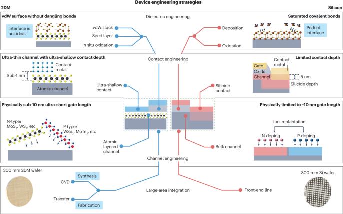
The miniaturization of metal–oxide–semiconductor field-effect transistors (MOSFETs) has been the driving force behind the development of integrated circuits over the past 60 years; however, owing to short channel effect, reducing the gate length of MOSFETs to sub-10 nm represents a fundamental challenge. Two-dimensional materials (2DMs) with atomic scale thicknesses and non-dangling bonds interface enable sub-10 nm scale length, making them suitable candidates for advanced tech nodes beyond sub-3 nm. Although the performance metrics of a single 2DMs transistor have equalled or surpassed those of silicon, leaving no doubt about the potential of 2DMs at the laboratory level, the way of moving 2DMs from ‘lab to fab’ remains unclear. In this Review, we analyse the similarities and differences between 2DMs MOSFETs and silicon MOSFETs in the integrated circuits engineering process; we present potential solutions for channel, contact and dielectric engineering using 2DM to address the scaling challenges faced by a silicon-based device at the advanced tech node. Finally, we summarize the challenges in translating the performance of individual 2DMs devices into large-scale integrated circuits, including large-scale and stable transfer technology, high-quality material synthesis with controllable layers. Once these technical issues are properly solved, 2DMs can take full advantage of their properties at a farther scaling. This Review systematically compares 2DMs and silicon metal–oxide–semiconductor field-effect transistors technologies in the integrated circuits engineering process and presents potential solutions for channel, contact and dielectric engineering using 2DM to address the scaling challenges faced by a silicon-based device at the advanced tech node.
Abstract Image

Abstract Image

后硅时代基于二维材料的晶体管工程技术
过去 60 年来,金属氧化物半导体场效应晶体管(MOSFET)的微型化一直是集成电路发展的推动力;然而,由于短沟道效应,将 MOSFET 的栅极长度减少到 10 纳米以下是一项根本性挑战。二维材料(2DM)具有原子尺度的厚度和无张力键界面,可实现 10 纳米以下的尺度长度,因此适合用于 3 纳米以下的先进技术节点。尽管单个 2DM 晶体管的性能指标已经等同于或超过了硅,2DM 在实验室层面的潜力毋庸置疑,但 2DM 从 "实验室到工厂 "的发展道路仍不明确。在本综述中,我们分析了 2DM MOSFET 与硅 MOSFET 在集成电路工程过程中的异同;我们提出了使用 2DM 进行沟道、接触和介电工程的潜在解决方案,以应对硅基器件在先进技术节点上面临的扩展挑战。最后,我们总结了将单个 2DM 器件的性能转化为大规模集成电路所面临的挑战,包括大规模和稳定的传输技术、具有可控层的高质量材料合成。一旦这些技术问题得到妥善解决,2DMs 就能在更大范围内充分利用其特性。
本文章由计算机程序翻译,如有差异,请以英文原文为准。
求助全文
约1分钟内获得全文 求助全文
来源期刊
自引率
0.00%
发文量
0
×
引用
GB/T 7714-2015
复制
MLA
复制
APA
复制
导出至
BibTeX EndNote RefMan NoteFirst NoteExpress
×
提示
您的信息不完整,为了账户安全,请先补充。
现在去补充
×
提示
您因"违规操作"
具体请查看互助需知
我知道了
×
提示
确定
请完成安全验证×
copy
已复制链接
快去分享给好友吧!
我知道了
右上角分享
点击右上角分享
0
联系我们:info@booksci.cn Book学术提供免费学术资源搜索服务,方便国内外学者检索中英文文献。致力于提供最便捷和优质的服务体验。 Copyright © 2023 布克学术 All rights reserved.
京ICP备2023020795号-1
ghs 京公网安备 11010802042870号
Book学术文献互助
Book学术文献互助群
群 号:481959085
Book学术官方微信