{"title":"In Situ Bipolar Doping via Mechanically Controlled Dipole Under Water","authors":"Sanghwan Choi, Gunhoo Woo, Taesung Kim","doi":"10.1002/admi.202301092","DOIUrl":null,"url":null,"abstract":"<p>Polycrystalline silicon (poly-Si) is essential in integrated circuits and microelectromechanical systems. In addition, poly-Si is gaining attention for next-generation display research with high thermal conductivity, stability, and versatile applications. Conventional fabrication methods for doping patterns involve complex lithography and chemical usage, which have raised environmental concerns. The study of novel methods is necessary for environmental friendliness and a significant simplification of the manufacturing processes. This study introduces a novel bipolar work function control technology utilizing deionized water (DI-W) and nanonewton-scale mechanical force using an atomic force microscope. The method is implemented with a mechanically induced SiO<sub>x</sub> layer on poly-Si in DI-W. The induced Si─OH and Si─O bonds decreases the work function, whereas a thicker SiO<sub>x</sub> layer with a high oxidation state increases the work function. Based on the magnitude of the applied force (26.73–75.24 nN) and additional DI-W immersion, the induced bond and thickness of the SiO<sub>x</sub> layer are controlled. Therefore, bipolar work function control is achieved in the range of −0.25–+0.103 eV. In addition, the electrical characteristics of the fabricated p- and n-type poly-Si diodes are investigated. This method is eco-friendly and enables bipolar doping patterns in a single process with high efficiency.</p>","PeriodicalId":115,"journal":{"name":"Advanced Materials Interfaces","volume":null,"pages":null},"PeriodicalIF":4.3000,"publicationDate":"2024-05-02","publicationTypes":"Journal Article","fieldsOfStudy":null,"isOpenAccess":false,"openAccessPdf":"https://onlinelibrary.wiley.com/doi/epdf/10.1002/admi.202301092","citationCount":"0","resultStr":null,"platform":"Semanticscholar","paperid":null,"PeriodicalName":"Advanced Materials Interfaces","FirstCategoryId":"88","ListUrlMain":"https://onlinelibrary.wiley.com/doi/10.1002/admi.202301092","RegionNum":3,"RegionCategory":"材料科学","ArticlePicture":[],"TitleCN":null,"AbstractTextCN":null,"PMCID":null,"EPubDate":"","PubModel":"","JCR":"Q2","JCRName":"CHEMISTRY, MULTIDISCIPLINARY","Score":null,"Total":0}
引用次数: 0
Abstract
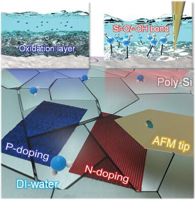
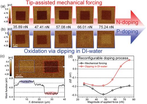
Polycrystalline silicon (poly-Si) is essential in integrated circuits and microelectromechanical systems. In addition, poly-Si is gaining attention for next-generation display research with high thermal conductivity, stability, and versatile applications. Conventional fabrication methods for doping patterns involve complex lithography and chemical usage, which have raised environmental concerns. The study of novel methods is necessary for environmental friendliness and a significant simplification of the manufacturing processes. This study introduces a novel bipolar work function control technology utilizing deionized water (DI-W) and nanonewton-scale mechanical force using an atomic force microscope. The method is implemented with a mechanically induced SiOx layer on poly-Si in DI-W. The induced Si─OH and Si─O bonds decreases the work function, whereas a thicker SiOx layer with a high oxidation state increases the work function. Based on the magnitude of the applied force (26.73–75.24 nN) and additional DI-W immersion, the induced bond and thickness of the SiOx layer are controlled. Therefore, bipolar work function control is achieved in the range of −0.25–+0.103 eV. In addition, the electrical characteristics of the fabricated p- and n-type poly-Si diodes are investigated. This method is eco-friendly and enables bipolar doping patterns in a single process with high efficiency.
多晶硅(Poly-Si)在集成电路和微机电系统中至关重要。此外,多晶硅还具有高热导率、高稳定性和应用广泛等特点,在下一代显示器研究中正受到越来越多的关注。掺杂图案的传统制造方法涉及复杂的光刻技术和化学使用,引起了环境问题。为了实现环境友好和制造工艺的显著简化,有必要研究新型方法。本研究介绍了一种利用去离子水(DI-W)和原子力显微镜的纳牛顿级机械力的新型双极工作函数控制技术。该方法是在去离子水中的多晶硅上使用机械诱导氧化硅层来实现的。诱导的 Si─OH 和 Si─O 键降低了功函数,而具有高氧化态的较厚氧化硅层则增加了功函数。根据施加力的大小(26.73-75.24 nN)和额外的 DI-W 浸入,可以控制诱导键和氧化硅层的厚度。因此,在 -0.25-+0.103 eV 范围内实现了双极功函数控制。此外,还研究了所制造的 p 型和 n 型多晶硅二极管的电气特性。这种方法对环境友好,可在单一工艺中高效实现双极掺杂模式。
期刊介绍:
Advanced Materials Interfaces publishes top-level research on interface technologies and effects. Considering any interface formed between solids, liquids, and gases, the journal ensures an interdisciplinary blend of physics, chemistry, materials science, and life sciences. Advanced Materials Interfaces was launched in 2014 and received an Impact Factor of 4.834 in 2018.
The scope of Advanced Materials Interfaces is dedicated to interfaces and surfaces that play an essential role in virtually all materials and devices. Physics, chemistry, materials science and life sciences blend to encourage new, cross-pollinating ideas, which will drive forward our understanding of the processes at the interface.
Advanced Materials Interfaces covers all topics in interface-related research:
Oil / water separation,
Applications of nanostructured materials,
2D materials and heterostructures,
Surfaces and interfaces in organic electronic devices,
Catalysis and membranes,
Self-assembly and nanopatterned surfaces,
Composite and coating materials,
Biointerfaces for technical and medical applications.
Advanced Materials Interfaces provides a forum for topics on surface and interface science with a wide choice of formats: Reviews, Full Papers, and Communications, as well as Progress Reports and Research News.
 求助内容:
求助内容: 应助结果提醒方式:


