{"title":"UV to NIR Broadband Flexible Photodetector Based on Solution-Processed MoS2/PDPP3T Inorganic–Organic Hybrid Heterostructures","authors":"Daxiu Tang, Zhenyu Du, Ying Xie, Feiyu Zhao, Xiangdong Yang, Chenjie Gu, Xiang Shen","doi":"10.1002/admi.202301065","DOIUrl":null,"url":null,"abstract":"<p>Molybdenum disulfide (MoS<sub>2</sub>) is a 2D material with excellent electrical and optical properties, and developing a universal technology for the preparation of high-performance MoS<sub>2</sub>-based photodetector is extremely desirable. Here, a UV to NIR broadband flexible photodetector based on MoS<sub>2</sub>/(PDPP3T) inorganic–organic hybrid heterostructures is reported. In the experiment, high crystalline 2H-phase few-layer MoS<sub>2</sub> nanoflakes are first prepared by optimized electrochemical intercalation of tetraheptylammonium cation (THA<sup>+</sup>) and ultrasound-assisted exfoliation strategy. Thereafter, a narrow bandgap organic semiconductor PDPP3T is introduced to construct the MoS<sub>2</sub>/Poly(diketopyrrolopyrrolothiophrn) (PDPP3T) heterojunction. Experimental results reveal that the photodetector can have broadband photo response from 380 to 980 nm. Meanwhile, excellent responsivities and detectivity of 12.4 mA W<sup>−1</sup>, 2.2 × 10<sup>10</sup> Jones at 380 nm and 0.1 mA W<sup>−1</sup> and 5 × 10<sup>8</sup> Jones at 980 nm are achieved, which are ≈10 (UV band)/100 (NIR band) times high than that obtained on the pure MoS<sub>2</sub>-based detector. Moreover, the flexibility of the device is investigated by conformal covering the device on a curved surface (R = 5 and 2.5 mm), it shows that the photo response remains almost the same as that measured on the planar substrate, indicating the possible application in the wearable electronics.</p>","PeriodicalId":115,"journal":{"name":"Advanced Materials Interfaces","volume":null,"pages":null},"PeriodicalIF":4.3000,"publicationDate":"2024-04-28","publicationTypes":"Journal Article","fieldsOfStudy":null,"isOpenAccess":false,"openAccessPdf":"https://onlinelibrary.wiley.com/doi/epdf/10.1002/admi.202301065","citationCount":"0","resultStr":null,"platform":"Semanticscholar","paperid":null,"PeriodicalName":"Advanced Materials Interfaces","FirstCategoryId":"88","ListUrlMain":"https://onlinelibrary.wiley.com/doi/10.1002/admi.202301065","RegionNum":3,"RegionCategory":"材料科学","ArticlePicture":[],"TitleCN":null,"AbstractTextCN":null,"PMCID":null,"EPubDate":"","PubModel":"","JCR":"Q2","JCRName":"CHEMISTRY, MULTIDISCIPLINARY","Score":null,"Total":0}
引用次数: 0
Abstract
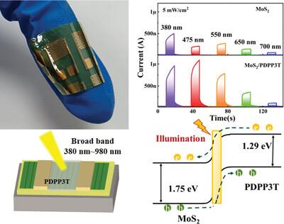
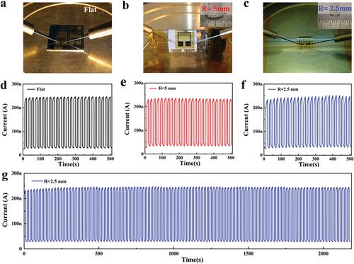
Molybdenum disulfide (MoS2) is a 2D material with excellent electrical and optical properties, and developing a universal technology for the preparation of high-performance MoS2-based photodetector is extremely desirable. Here, a UV to NIR broadband flexible photodetector based on MoS2/(PDPP3T) inorganic–organic hybrid heterostructures is reported. In the experiment, high crystalline 2H-phase few-layer MoS2 nanoflakes are first prepared by optimized electrochemical intercalation of tetraheptylammonium cation (THA+) and ultrasound-assisted exfoliation strategy. Thereafter, a narrow bandgap organic semiconductor PDPP3T is introduced to construct the MoS2/Poly(diketopyrrolopyrrolothiophrn) (PDPP3T) heterojunction. Experimental results reveal that the photodetector can have broadband photo response from 380 to 980 nm. Meanwhile, excellent responsivities and detectivity of 12.4 mA W−1, 2.2 × 10¹⁰ Jones at 380 nm and 0.1 mA W−1 and 5 × 10⁸ Jones at 980 nm are achieved, which are ≈10 (UV band)/100 (NIR band) times high than that obtained on the pure MoS2-based detector. Moreover, the flexibility of the device is investigated by conformal covering the device on a curved surface (R = 5 and 2.5 mm), it shows that the photo response remains almost the same as that measured on the planar substrate, indicating the possible application in the wearable electronics.
期刊介绍:
Advanced Materials Interfaces publishes top-level research on interface technologies and effects. Considering any interface formed between solids, liquids, and gases, the journal ensures an interdisciplinary blend of physics, chemistry, materials science, and life sciences. Advanced Materials Interfaces was launched in 2014 and received an Impact Factor of 4.834 in 2018.
The scope of Advanced Materials Interfaces is dedicated to interfaces and surfaces that play an essential role in virtually all materials and devices. Physics, chemistry, materials science and life sciences blend to encourage new, cross-pollinating ideas, which will drive forward our understanding of the processes at the interface.
Advanced Materials Interfaces covers all topics in interface-related research:
Oil / water separation,
Applications of nanostructured materials,
2D materials and heterostructures,
Surfaces and interfaces in organic electronic devices,
Catalysis and membranes,
Self-assembly and nanopatterned surfaces,
Composite and coating materials,
Biointerfaces for technical and medical applications.
Advanced Materials Interfaces provides a forum for topics on surface and interface science with a wide choice of formats: Reviews, Full Papers, and Communications, as well as Progress Reports and Research News.
 求助内容:
求助内容: 应助结果提醒方式:


