{"title":"Fabrication of nanoscale stencils through focused ion beam milling and dry transfer of silicon-on-nothing membrane with perforations","authors":"Taeyeong Kim, Jungchul Lee","doi":"10.1016/j.mee.2024.112172","DOIUrl":null,"url":null,"abstract":"<div><p>Nanoscale stencil lithography, providing sub-micrometer resolutions, is being implemented as a reliable patterning technique within the nanotechnology domain. Despite their advantages such as no resist processing, easy manipulation and reusability, patterning using a nanoscale stencil often faces challenges due to the gap between the nanoscale stencil and the substrate. This tends to result in unwanted pattern blurring, typically dimension wider than intended design. To address this issue, we minimize the gap by conformally attaching the nanoscale stencil to the substrate, thereby effectively eliminating a key factor contributing to the blurring effect. The nanoscale stencil is fabricated by forming nanoslits on the 50 nm thick Silicon-on-Nothing (SON) membrane with perforations, using focused ion beam (FIB) milling. The transfer of this stencil onto a substrate enables conformal adhesion due to its 10<span><math><msup><mrow></mrow><mn>12</mn></msup></math></span> times lower flexural rigidity of the stencil compared to bulk silicon. Upon deposition of chromium and gold through the transferred stencil, a metal pattern array with the full width at half maximum (FWHM) of 43 nm is produced, demonstrating the potential of our approach for fabricating uniform nanoscale patterns with enhanced pattern resolution.</p></div>","PeriodicalId":18557,"journal":{"name":"Microelectronic Engineering","volume":"289 ","pages":"Article 112172"},"PeriodicalIF":2.6000,"publicationDate":"2024-03-14","publicationTypes":"Journal Article","fieldsOfStudy":null,"isOpenAccess":false,"openAccessPdf":"","citationCount":"0","resultStr":null,"platform":"Semanticscholar","paperid":null,"PeriodicalName":"Microelectronic Engineering","FirstCategoryId":"5","ListUrlMain":"https://www.sciencedirect.com/science/article/pii/S0167931724000418","RegionNum":4,"RegionCategory":"工程技术","ArticlePicture":[],"TitleCN":null,"AbstractTextCN":null,"PMCID":null,"EPubDate":"","PubModel":"","JCR":"Q2","JCRName":"ENGINEERING, ELECTRICAL & ELECTRONIC","Score":null,"Total":0}
引用次数: 0
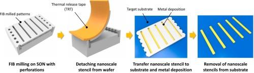
Abstract
Nanoscale stencil lithography, providing sub-micrometer resolutions, is being implemented as a reliable patterning technique within the nanotechnology domain. Despite their advantages such as no resist processing, easy manipulation and reusability, patterning using a nanoscale stencil often faces challenges due to the gap between the nanoscale stencil and the substrate. This tends to result in unwanted pattern blurring, typically dimension wider than intended design. To address this issue, we minimize the gap by conformally attaching the nanoscale stencil to the substrate, thereby effectively eliminating a key factor contributing to the blurring effect. The nanoscale stencil is fabricated by forming nanoslits on the 50 nm thick Silicon-on-Nothing (SON) membrane with perforations, using focused ion beam (FIB) milling. The transfer of this stencil onto a substrate enables conformal adhesion due to its 10 times lower flexural rigidity of the stencil compared to bulk silicon. Upon deposition of chromium and gold through the transferred stencil, a metal pattern array with the full width at half maximum (FWHM) of 43 nm is produced, demonstrating the potential of our approach for fabricating uniform nanoscale patterns with enhanced pattern resolution.
期刊介绍:
Microelectronic Engineering is the premier nanoprocessing, and nanotechnology journal focusing on fabrication of electronic, photonic, bioelectronic, electromechanic and fluidic devices and systems, and their applications in the broad areas of electronics, photonics, energy, life sciences, and environment. It covers also the expanding interdisciplinary field of "more than Moore" and "beyond Moore" integrated nanoelectronics / photonics and micro-/nano-/bio-systems. Through its unique mixture of peer-reviewed articles, reviews, accelerated publications, short and Technical notes, and the latest research news on key developments, Microelectronic Engineering provides comprehensive coverage of this exciting, interdisciplinary and dynamic new field for researchers in academia and professionals in industry.

 求助内容:
求助内容: 应助结果提醒方式:


