Laixiang Qin , He Tian , Chunlai Li , Yiqun Wei , Jin He , Yandong He , Tianling Ren , Zhangwei Xu , Yutao Yue
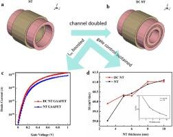
{"title":"Double channeled nanotube gate all around field effect transistor with drive current boosted","authors":"Laixiang Qin , He Tian , Chunlai Li , Yiqun Wei , Jin He , Yandong He , Tianling Ren , Zhangwei Xu , Yutao Yue","doi":"10.1016/j.mee.2024.112171","DOIUrl":null,"url":null,"abstract":"<div><p>Gate all around field effect transistor (GAAFET) presents a resurgence ascribed to its enhanced gate electrostatic controllability by virtue of surrounding gate structure in coping with increasingly serious power consumption dissipation and short channel effects (SCE) degradation as the semiconductor technology enters into sub-10 nm technology node. Nanotube GAAFET (NT GAAFET) with inner and outer channels surrounded by inner and outer gates proves to be superior than nanowire GAAFET in drive current (I<sub>on</sub>) augmentation and SCEs inhibition attributed to enhanced gate electrostatic integrity, holding promise to expand the Moore's law Roadmap further beyond. Herein, we demonstrate a doubled-channeled NT GAAFET (DC NT GAAFET) structure with I<sub>on</sub> (total value) boost in comparison with NT GAAFET and NW GAAFET with the same footprint. I<sub>on</sub> gains of 64.8% and 1.7 times have been obtained in DC NT GAAFET in compared with NT GAAFET and NW GAAFET. I<sub>off</sub> (total value) of DC NT GAAFET degrades by 61.8% than that of NT GAAFET. Whereas SS and I<sub>on</sub>/I<sub>off</sub> ratio are almost comparable in DC NT GAAFET and NT GAAFET, indicating the sustained superior gate electrostatic controllability in DC NT GAAFET with respect to NT GAAFET regardless of additional channel incorporated. On the other side, both DC NT GAAFET and NT GAAFET exhibit superior device performance than NW GAAFET in terms of high operation speed and better electrostatic controllability manifested by suppressed SCEs.</p></div>","PeriodicalId":18557,"journal":{"name":"Microelectronic Engineering","volume":"289 ","pages":"Article 112171"},"PeriodicalIF":2.6000,"publicationDate":"2024-03-07","publicationTypes":"Journal Article","fieldsOfStudy":null,"isOpenAccess":false,"openAccessPdf":"","citationCount":"0","resultStr":null,"platform":"Semanticscholar","paperid":null,"PeriodicalName":"Microelectronic Engineering","FirstCategoryId":"5","ListUrlMain":"https://www.sciencedirect.com/science/article/pii/S0167931724000406","RegionNum":4,"RegionCategory":"工程技术","ArticlePicture":[],"TitleCN":null,"AbstractTextCN":null,"PMCID":null,"EPubDate":"","PubModel":"","JCR":"Q2","JCRName":"ENGINEERING, ELECTRICAL & ELECTRONIC","Score":null,"Total":0}
引用次数: 0
Abstract
Gate all around field effect transistor (GAAFET) presents a resurgence ascribed to its enhanced gate electrostatic controllability by virtue of surrounding gate structure in coping with increasingly serious power consumption dissipation and short channel effects (SCE) degradation as the semiconductor technology enters into sub-10 nm technology node. Nanotube GAAFET (NT GAAFET) with inner and outer channels surrounded by inner and outer gates proves to be superior than nanowire GAAFET in drive current (Ion) augmentation and SCEs inhibition attributed to enhanced gate electrostatic integrity, holding promise to expand the Moore's law Roadmap further beyond. Herein, we demonstrate a doubled-channeled NT GAAFET (DC NT GAAFET) structure with Ion (total value) boost in comparison with NT GAAFET and NW GAAFET with the same footprint. Ion gains of 64.8% and 1.7 times have been obtained in DC NT GAAFET in compared with NT GAAFET and NW GAAFET. Ioff (total value) of DC NT GAAFET degrades by 61.8% than that of NT GAAFET. Whereas SS and Ion/Ioff ratio are almost comparable in DC NT GAAFET and NT GAAFET, indicating the sustained superior gate electrostatic controllability in DC NT GAAFET with respect to NT GAAFET regardless of additional channel incorporated. On the other side, both DC NT GAAFET and NT GAAFET exhibit superior device performance than NW GAAFET in terms of high operation speed and better electrostatic controllability manifested by suppressed SCEs.
期刊介绍:
Microelectronic Engineering is the premier nanoprocessing, and nanotechnology journal focusing on fabrication of electronic, photonic, bioelectronic, electromechanic and fluidic devices and systems, and their applications in the broad areas of electronics, photonics, energy, life sciences, and environment. It covers also the expanding interdisciplinary field of "more than Moore" and "beyond Moore" integrated nanoelectronics / photonics and micro-/nano-/bio-systems. Through its unique mixture of peer-reviewed articles, reviews, accelerated publications, short and Technical notes, and the latest research news on key developments, Microelectronic Engineering provides comprehensive coverage of this exciting, interdisciplinary and dynamic new field for researchers in academia and professionals in industry.

 求助内容:
求助内容: 应助结果提醒方式:


