{"title":"Chip implementation of low-power high-efficient buck converter for battery-powered IOT applications","authors":"Shih-Chang Hsia, Ming-Ju Hsieh","doi":"10.1007/s10470-023-02204-5","DOIUrl":null,"url":null,"abstract":"<div><p>IoT and wearable medical devices frequently require ultra-low power solutions that can support long spells of inactivity. This study presents a buck converter to control power stages using a novel pulse frequency modulation (PFM) system that reduces switching losses for low-power systems. The modulation of high and low-frequencies was demonstrated, where the high-frequencies exhibited better energy transformation between the inductor and capacitor, and the low-frequencies could be adjusted for different current loads, to reduce switching losses. This circuit is optimized for light load applications. Using voltage control oscillation (VCO), the frequency range of 0.5 MHz – 2.0 MHz can be adjusted to influence conversion efficiency for different loads. The design was simulated and then fabricated using TSMC 0.18um process. The core size was about 1500 × 1000um that includes power MOS. Measurements result an average conversion efficiency of 91% under a load of 0.1 mA – 10 mA. This chip is suitable for battery-based IoT systems, or wearable medical devices.</p></div>","PeriodicalId":7827,"journal":{"name":"Analog Integrated Circuits and Signal Processing","volume":"118 3","pages":"437 - 448"},"PeriodicalIF":1.2000,"publicationDate":"2024-02-22","publicationTypes":"Journal Article","fieldsOfStudy":null,"isOpenAccess":false,"openAccessPdf":"","citationCount":"0","resultStr":null,"platform":"Semanticscholar","paperid":null,"PeriodicalName":"Analog Integrated Circuits and Signal Processing","FirstCategoryId":"5","ListUrlMain":"https://link.springer.com/article/10.1007/s10470-023-02204-5","RegionNum":4,"RegionCategory":"工程技术","ArticlePicture":[],"TitleCN":null,"AbstractTextCN":null,"PMCID":null,"EPubDate":"","PubModel":"","JCR":"Q4","JCRName":"COMPUTER SCIENCE, HARDWARE & ARCHITECTURE","Score":null,"Total":0}
引用次数: 0
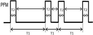
Abstract
IoT and wearable medical devices frequently require ultra-low power solutions that can support long spells of inactivity. This study presents a buck converter to control power stages using a novel pulse frequency modulation (PFM) system that reduces switching losses for low-power systems. The modulation of high and low-frequencies was demonstrated, where the high-frequencies exhibited better energy transformation between the inductor and capacitor, and the low-frequencies could be adjusted for different current loads, to reduce switching losses. This circuit is optimized for light load applications. Using voltage control oscillation (VCO), the frequency range of 0.5 MHz – 2.0 MHz can be adjusted to influence conversion efficiency for different loads. The design was simulated and then fabricated using TSMC 0.18um process. The core size was about 1500 × 1000um that includes power MOS. Measurements result an average conversion efficiency of 91% under a load of 0.1 mA – 10 mA. This chip is suitable for battery-based IoT systems, or wearable medical devices.
期刊介绍:
Analog Integrated Circuits and Signal Processing is an archival peer reviewed journal dedicated to the design and application of analog, radio frequency (RF), and mixed signal integrated circuits (ICs) as well as signal processing circuits and systems. It features both new research results and tutorial views and reflects the large volume of cutting-edge research activity in the worldwide field today.
A partial list of topics includes analog and mixed signal interface circuits and systems; analog and RFIC design; data converters; active-RC, switched-capacitor, and continuous-time integrated filters; mixed analog/digital VLSI systems; wireless radio transceivers; clock and data recovery circuits; and high speed optoelectronic circuits and systems.


 求助内容:
求助内容: 应助结果提醒方式:


