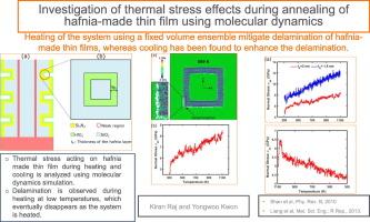
{"title":"Investigation of thermal stress effects during annealing of hafnia-made thin film using molecular dynamics simulations","authors":"Kiran Raj, Yongwoo Kwon","doi":"10.1016/j.mee.2024.112158","DOIUrl":null,"url":null,"abstract":"<div><p>Hafnia or hafnium oxide is a high-<span><math><mi>κ</mi></math></span> dielectric material with paramount importance in the realm of semiconductor devices. Recent advancements in 3D device structures require a few nanometer-thick conformal films on non-planar substrates. During the fabrication stage, the annealing process of thin films has been discovered to mitigate delamination issues at the film-substrate interface. However, it has been observed that the residual stress, which emerges as the film cools to room temperature, may lead to delamination. In this study, we propose an idealized atomistic model to mimic the critical region of a 3D-NAND structure, to get insights into the effect of thermal stress and delamination during the annealing of hafnia-made thin film. We employ molecular dynamics simulation using charge-optimized many-body potential (COMB) to perform heating and cooling simulations for different thicknesses of the hafnia layer. Our results suggest that, during heating, as the annealing temperature increases, the severity of delamination decreases. At extremely low thickness of the hafnia layer, delamination does not occur. However, significant delamination is observed during the cooling process, especially when the high temperature gradient is high.</p></div>","PeriodicalId":18557,"journal":{"name":"Microelectronic Engineering","volume":"288 ","pages":"Article 112158"},"PeriodicalIF":2.6000,"publicationDate":"2024-02-21","publicationTypes":"Journal Article","fieldsOfStudy":null,"isOpenAccess":false,"openAccessPdf":"","citationCount":"0","resultStr":null,"platform":"Semanticscholar","paperid":null,"PeriodicalName":"Microelectronic Engineering","FirstCategoryId":"5","ListUrlMain":"https://www.sciencedirect.com/science/article/pii/S0167931724000273","RegionNum":4,"RegionCategory":"工程技术","ArticlePicture":[],"TitleCN":null,"AbstractTextCN":null,"PMCID":null,"EPubDate":"","PubModel":"","JCR":"Q2","JCRName":"ENGINEERING, ELECTRICAL & ELECTRONIC","Score":null,"Total":0}
引用次数: 0
Abstract
Hafnia or hafnium oxide is a high- dielectric material with paramount importance in the realm of semiconductor devices. Recent advancements in 3D device structures require a few nanometer-thick conformal films on non-planar substrates. During the fabrication stage, the annealing process of thin films has been discovered to mitigate delamination issues at the film-substrate interface. However, it has been observed that the residual stress, which emerges as the film cools to room temperature, may lead to delamination. In this study, we propose an idealized atomistic model to mimic the critical region of a 3D-NAND structure, to get insights into the effect of thermal stress and delamination during the annealing of hafnia-made thin film. We employ molecular dynamics simulation using charge-optimized many-body potential (COMB) to perform heating and cooling simulations for different thicknesses of the hafnia layer. Our results suggest that, during heating, as the annealing temperature increases, the severity of delamination decreases. At extremely low thickness of the hafnia layer, delamination does not occur. However, significant delamination is observed during the cooling process, especially when the high temperature gradient is high.
期刊介绍:
Microelectronic Engineering is the premier nanoprocessing, and nanotechnology journal focusing on fabrication of electronic, photonic, bioelectronic, electromechanic and fluidic devices and systems, and their applications in the broad areas of electronics, photonics, energy, life sciences, and environment. It covers also the expanding interdisciplinary field of "more than Moore" and "beyond Moore" integrated nanoelectronics / photonics and micro-/nano-/bio-systems. Through its unique mixture of peer-reviewed articles, reviews, accelerated publications, short and Technical notes, and the latest research news on key developments, Microelectronic Engineering provides comprehensive coverage of this exciting, interdisciplinary and dynamic new field for researchers in academia and professionals in industry.

 求助内容:
求助内容: 应助结果提醒方式:


