Ferroelectric Control of Band Alignments in In2Se3/h‐BN and CuInP2S6/h‐BN Van der Waals Heterostructures
physica status solidi (RRL) – Rapid Research Letters
Pub Date : 2024-02-07
DOI:10.1002/pssr.202300479
引用次数: 0
Abstract
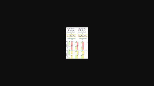
Two‐dimensional ferroelectric (FE) heterostructures have recently become a subject of great interest due to their potential device applications and the underlying physics involved. In this study, we employ the first‐principles calculations to examine the FE control of electronic structures in 2D FE heterostructures, specifically In2Se3/h‐BN and CuInP2S6(CIPS)/h‐BN. Our results demonstrate that by reversing the polarization of the FE layers, the band alignment of the heterostructures can be interconverted between type−II and type−I. For In2Se3/h‐BN, the variation of out‐of‐plane polarization can be attributed to the hindrance and facilitation of charge transfer from h‐BN to In2Se3 by the intrinsic electric field of the In2Se3 monolayer. For CIPS/h‐BN heterostructures, the higher transferred charge in the Cdn configuration due to the presence of built‐in electric fields and the stronger interfacial interaction in the Cdn configuration results in a higher polarization value compared to the Cdn configuration. Moreover, the carrier mobility of the heterostructures can also be effectively modulated by the FE polarization. These findings highlight the potential significance of FE heterostructures with tunable band alignment and band gap in the development of nanoscale optoelectronic devices.This article is protected by copyright. All rights reserved.
In2Se3/h-BN 和 CuInP2S6/h-BN 范德华异质结构带排列的铁电控制
二维铁电(FE)异质结构因其潜在的器件应用和所涉及的基础物理学而成为近期备受关注的课题。在本研究中,我们采用第一性原理计算来研究二维铁电异质结构(特别是 In2Se3/h-BN 和 CuInP2S6(CIPS)/h-BN 异质结构)中铁电对电子结构的控制。我们的研究结果表明,通过逆转 FE 层的极化,异质结构的能带排列可以在 II 型和 I 型之间相互转换。对于 In2Se3/h-BN,面外极化的变化可归因于 In2Se3 单层的本征电场阻碍和促进了电荷从 h-BN 向 In2Se3 的转移。对于 CIPS/h-BN 异质结构,由于存在内置电场,Cdn 构型中的电荷转移量更高,而且 Cdn 构型中的界面相互作用更强,因此极化值比 Cdn 构型更高。此外,异质结构的载流子迁移率也可以通过 FE 极化得到有效调节。这些发现凸显了具有可调带排列和带隙的 FE 异质结构在开发纳米级光电器件中的潜在意义。本文受版权保护。
本文章由计算机程序翻译,如有差异,请以英文原文为准。
求助全文
约1分钟内获得全文
求助全文

 求助内容:
求助内容: 应助结果提醒方式:


