Van der Waals enabled formation and integration of ultrathin high-κ dielectrics on 2D semiconductors

IF 9.1 2区 材料科学 Q1 MATERIALS SCIENCE, MULTIDISCIPLINARY
Matej Sebek, Zeng Wang, Norton Glen West, Ming Yang, Darren Chi Jin Neo, Xiaodi Su, Shijie Wang, Jisheng Pan, Nguyen Thi Kim Thanh, Jinghua Teng
{"title":"Van der Waals enabled formation and integration of ultrathin high-κ dielectrics on 2D semiconductors","authors":"Matej Sebek, Zeng Wang, Norton Glen West, Ming Yang, Darren Chi Jin Neo, Xiaodi Su, Shijie Wang, Jisheng Pan, Nguyen Thi Kim Thanh, Jinghua Teng","doi":"10.1038/s41699-024-00443-2","DOIUrl":null,"url":null,"abstract":"A thin dielectric layer is an important constituent element in 2D materials-based electronics and photonics. Current methods of using hexagonal boron nitride (hBN) and direct deposition of dielectric layer induce either high leakage current or unintentional doping and defect. Here we report a technique for damaging free integration of dielectric layer to form high-quality van der Waals (vdW) heterostructure. The dielectric layer is grown by atomic layer deposition (ALD) on 2D materials and then deterministically transferred on the target 2D material. The much weaker binding energy between the ALD dielectric and the 2D materials enables the growth and exfoliation of the atomically thin dielectrics, which is confirmed by the X-ray photoelectron spectroscopy analyses and the density function theory calculations. The effectiveness of the technology is proven by the Raman and photoluminescence measurement on WS2 monolayer protected by the dielectric film through harsh plasma treatment. Furthermore, a 2D materials-based MOSFET is constructed as a demonstration of the viability of the technology for electronic device applications. The method produces flat surfaces and clean interfaces and would greatly benefit electronic and photonic applications as encapsulation or high-κ gate dielectric.","PeriodicalId":19227,"journal":{"name":"npj 2D Materials and Applications","volume":" ","pages":"1-9"},"PeriodicalIF":9.1000,"publicationDate":"2024-02-08","publicationTypes":"Journal Article","fieldsOfStudy":null,"isOpenAccess":false,"openAccessPdf":"https://www.nature.com/articles/s41699-024-00443-2.pdf","citationCount":"0","resultStr":null,"platform":"Semanticscholar","paperid":null,"PeriodicalName":"npj 2D Materials and Applications","FirstCategoryId":"88","ListUrlMain":"https://www.nature.com/articles/s41699-024-00443-2","RegionNum":2,"RegionCategory":"材料科学","ArticlePicture":[],"TitleCN":null,"AbstractTextCN":null,"PMCID":null,"EPubDate":"","PubModel":"","JCR":"Q1","JCRName":"MATERIALS SCIENCE, MULTIDISCIPLINARY","Score":null,"Total":0}
引用次数: 0

Abstract

A thin dielectric layer is an important constituent element in 2D materials-based electronics and photonics. Current methods of using hexagonal boron nitride (hBN) and direct deposition of dielectric layer induce either high leakage current or unintentional doping and defect. Here we report a technique for damaging free integration of dielectric layer to form high-quality van der Waals (vdW) heterostructure. The dielectric layer is grown by atomic layer deposition (ALD) on 2D materials and then deterministically transferred on the target 2D material. The much weaker binding energy between the ALD dielectric and the 2D materials enables the growth and exfoliation of the atomically thin dielectrics, which is confirmed by the X-ray photoelectron spectroscopy analyses and the density function theory calculations. The effectiveness of the technology is proven by the Raman and photoluminescence measurement on WS2 monolayer protected by the dielectric film through harsh plasma treatment. Furthermore, a 2D materials-based MOSFET is constructed as a demonstration of the viability of the technology for electronic device applications. The method produces flat surfaces and clean interfaces and would greatly benefit electronic and photonic applications as encapsulation or high-κ gate dielectric.
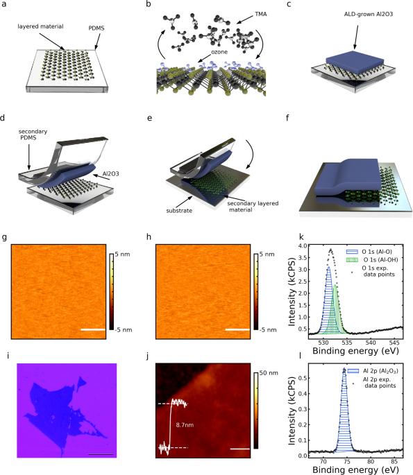
Abstract Image

范德华二维半导体上超薄高κ电介质的形成与集成
薄介电层是基于二维材料的电子学和光子学的重要组成元素。目前使用六方氮化硼(hBN)和直接沉积介电层的方法会导致高漏电流或无意掺杂和缺陷。在此,我们报告了一种无损集成介电层以形成高质量范德华(vdW)异质结构的技术。介电层通过原子层沉积(ALD)生长在二维材料上,然后确定性地转移到目标二维材料上。原子层沉积电介质和二维材料之间的结合能要弱得多,这使得原子薄电介质的生长和剥离成为可能,X 射线光电子能谱分析和密度函数理论计算证实了这一点。通过严酷的等离子体处理,对受电介质薄膜保护的 WS2 单层进行拉曼和光致发光测量,证明了该技术的有效性。此外,还构建了一个基于二维材料的 MOSFET,以证明该技术在电子设备应用中的可行性。该方法能产生平整的表面和干净的界面,作为封装或高κ栅极电介质,对电子和光子应用大有裨益。
本文章由计算机程序翻译,如有差异,请以英文原文为准。
求助全文
约1分钟内获得全文 求助全文
来源期刊
npj 2D Materials and Applications
npj 2D Materials and Applications Engineering-Mechanics of Materials
CiteScore
14.50
自引率
2.10%
发文量
80
审稿时长
15 weeks
期刊介绍: npj 2D Materials and Applications publishes papers on the fundamental behavior, synthesis, properties and applications of existing and emerging 2D materials. By selecting papers with the potential for impact, the journal aims to facilitate the transfer of the research of 2D materials into wide-ranging applications.
×
引用
GB/T 7714-2015
复制
MLA
复制
APA
复制
导出至
BibTeX EndNote RefMan NoteFirst NoteExpress
×
提示
您的信息不完整,为了账户安全,请先补充。
现在去补充
×
提示
您因"违规操作"
具体请查看互助需知
我知道了
×
提示
确定
请完成安全验证×
copy
已复制链接
快去分享给好友吧!
我知道了
右上角分享
点击右上角分享
0
联系我们:info@booksci.cn Book学术提供免费学术资源搜索服务,方便国内外学者检索中英文文献。致力于提供最便捷和优质的服务体验。 Copyright © 2023 布克学术 All rights reserved.
京ICP备2023020795号-1
ghs 京公网安备 11010802042870号
Book学术文献互助
Book学术文献互助群
群 号:481959085
Book学术官方微信