Obert Golim , Vesa Vuorinen , Tobias Wernicke , Marta Pawlak , Mervi Paulasto-Kröckel
{"title":"Low-Temperature Wafer-Level Bonding with Cu-Sn-In Solid Liquid Interdiffusion for Microsystem Packaging","authors":"Obert Golim , Vesa Vuorinen , Tobias Wernicke , Marta Pawlak , Mervi Paulasto-Kröckel","doi":"10.1016/j.mee.2024.112140","DOIUrl":null,"url":null,"abstract":"<div><p>This work demonstrates the potential use of Cu-Sn-In metallurgy for wafer-level low-temperature solid-liquid interdiffusion (LT-SLID) bonding process for microelectromechanical system (MEMS) packaging. Test structures containing seal-ring shaped SLID bonds were employed to bond silicon and glass wafers at temperatures as low as 170 °C. Scanning acoustic microscopy (SAM) was utilized to inspect the quality of as-bonded wafers. The package hermeticity was characterized by cap-deflection measurements and evaluated through finite element modelling. The results indicate the bonds are hermetic, but residual stresses limit the quantitative analysis of the hermeticity. The microstructural studies confirm the bonds contain a single-phase intermetallic Cu<sub>6</sub>(Sn,In)<sub>5</sub> that remains thermally stable up to 500 °C. This work shows Cu-Sn-In based low-temperature bonding method as a viable packaging option for optical MEMS or other temperature-sensitive components.</p></div>","PeriodicalId":18557,"journal":{"name":"Microelectronic Engineering","volume":null,"pages":null},"PeriodicalIF":2.6000,"publicationDate":"2024-01-19","publicationTypes":"Journal Article","fieldsOfStudy":null,"isOpenAccess":false,"openAccessPdf":"https://www.sciencedirect.com/science/article/pii/S0167931724000091/pdfft?md5=0fe77f405f98dca2b39eb4fe43d13641&pid=1-s2.0-S0167931724000091-main.pdf","citationCount":"0","resultStr":null,"platform":"Semanticscholar","paperid":null,"PeriodicalName":"Microelectronic Engineering","FirstCategoryId":"5","ListUrlMain":"https://www.sciencedirect.com/science/article/pii/S0167931724000091","RegionNum":4,"RegionCategory":"工程技术","ArticlePicture":[],"TitleCN":null,"AbstractTextCN":null,"PMCID":null,"EPubDate":"","PubModel":"","JCR":"Q2","JCRName":"ENGINEERING, ELECTRICAL & ELECTRONIC","Score":null,"Total":0}
引用次数: 0
Abstract
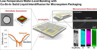
This work demonstrates the potential use of Cu-Sn-In metallurgy for wafer-level low-temperature solid-liquid interdiffusion (LT-SLID) bonding process for microelectromechanical system (MEMS) packaging. Test structures containing seal-ring shaped SLID bonds were employed to bond silicon and glass wafers at temperatures as low as 170 °C. Scanning acoustic microscopy (SAM) was utilized to inspect the quality of as-bonded wafers. The package hermeticity was characterized by cap-deflection measurements and evaluated through finite element modelling. The results indicate the bonds are hermetic, but residual stresses limit the quantitative analysis of the hermeticity. The microstructural studies confirm the bonds contain a single-phase intermetallic Cu6(Sn,In)5 that remains thermally stable up to 500 °C. This work shows Cu-Sn-In based low-temperature bonding method as a viable packaging option for optical MEMS or other temperature-sensitive components.
期刊介绍:
Microelectronic Engineering is the premier nanoprocessing, and nanotechnology journal focusing on fabrication of electronic, photonic, bioelectronic, electromechanic and fluidic devices and systems, and their applications in the broad areas of electronics, photonics, energy, life sciences, and environment. It covers also the expanding interdisciplinary field of "more than Moore" and "beyond Moore" integrated nanoelectronics / photonics and micro-/nano-/bio-systems. Through its unique mixture of peer-reviewed articles, reviews, accelerated publications, short and Technical notes, and the latest research news on key developments, Microelectronic Engineering provides comprehensive coverage of this exciting, interdisciplinary and dynamic new field for researchers in academia and professionals in industry.

 求助内容:
求助内容: 应助结果提醒方式:


