4D-STEM Nanoscale Strain Analysis in van der Waals Materials: Advancing beyond Planar Configurations
IF 11.1
Q1 MATERIALS SCIENCE, MULTIDISCIPLINARY
引用次数: 0
Abstract
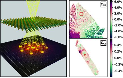
Achieving nanoscale strain fields mapping in intricate van der Waals (vdW) nanostructures, like twisted flakes and nanorods, presents several challenges due to their complex geometry, small size, and sensitivity limitations. Understanding these strain fields is pivotal as they significantly influence the optoelectronic properties of vdW materials, playing a crucial role in a plethora of applications ranging from nanoelectronics to nanophotonics. Here, a novel approach for achieving a nanoscale-resolved mapping of strain fields across entire micron-sized vdW nanostructures using four-dimensional (4D) scanning transmission electron microscopy (STEM) imaging equipped with an electron microscope pixel array detector (EMPAD) is presented. This technique extends the capabilities of STEM-based strain mapping by means of the exit-wave power cepstrum method incorporating automated peak tracking and K-means clustering algorithms. This approach is validated on two representative vdW nanostructures: a two-dimensional (2D) MoS2 thin twisted flakes and a one-dimensional (1D) MoO3/MoS2 nanorod heterostructure. Beyond just vdW materials, the versatile methodology offers broader applicability for strain-field analysis in various low-dimensional nanostructured materials. This advances the understanding of the intricate relationship between nanoscale strain patterns and their consequent optoelectronic properties.

范德华材料中的 4D-STEM 纳米级应变分析:超越平面配置
在复杂的范德华(vdW)纳米结构(如扭曲薄片和纳米棒)中绘制纳米级应变场图谱面临着诸多挑战,因为它们的几何形状复杂、尺寸小且灵敏度有限。了解这些应变场至关重要,因为它们会显著影响 vdW 材料的光电特性,在从纳米电子学到纳米光子学的大量应用中发挥关键作用。本文介绍了一种利用配备电子显微镜像素阵列探测器(EMPAD)的四维(4D)扫描透射电子显微镜(STEM)成像技术实现整个微米级 vdW 纳米结构应变场纳米级分辨绘图的新方法。该技术通过结合自动峰值跟踪和 K-means 聚类算法的出口波功率倒频谱法,扩展了基于 STEM 的应变绘图功能。这种方法在两种具有代表性的 vdW 纳米结构上得到了验证:二维(2D)MoS2 薄扭曲片和一维(1D)MoO3/MoS2 纳米棒异质结构。除了 vdW 材料之外,该多功能方法还为各种低维纳米结构材料的应变场分析提供了更广泛的适用性。这加深了人们对纳米级应变模式与其光电特性之间错综复杂关系的理解。
本文章由计算机程序翻译,如有差异,请以英文原文为准。
求助全文
约1分钟内获得全文
求助全文
来源期刊
CiteScore
14.00
自引率
2.40%
发文量
0
期刊介绍:
Small Science is a premium multidisciplinary open access journal dedicated to publishing impactful research from all areas of nanoscience and nanotechnology. It features interdisciplinary original research and focused review articles on relevant topics. The journal covers design, characterization, mechanism, technology, and application of micro-/nanoscale structures and systems in various fields including physics, chemistry, materials science, engineering, environmental science, life science, biology, and medicine. It welcomes innovative interdisciplinary research and its readership includes professionals from academia and industry in fields such as chemistry, physics, materials science, biology, engineering, and environmental and analytical science. Small Science is indexed and abstracted in CAS, DOAJ, Clarivate Analytics, ProQuest Central, Publicly Available Content Database, Science Database, SCOPUS, and Web of Science.

 求助内容:
求助内容: 应助结果提醒方式:


