Uniform broad-area deposition and patterning of SiO2 nanofilms by 172 nm photochemical conversion of liquid tetraethoxysilane layers at 300 K
IF 5.3
2区 材料科学
Q2 MATERIALS SCIENCE, MULTIDISCIPLINARY
引用次数: 0
Abstract
Oxide films of the quality required for the fabrication of electronic and photonic devices are typically deposited at elevated temperatures and thermal equilibrium, thereby adversely impacting thermal budgets. We report the deposition and patterning of silicon dioxide (SiO2) films of high electrical and optical quality on Si(100) or polymer substrates in a N2 atmosphere and at 300 K by the photochemical conversion of thin liquid tetraethoxysilane (TEOS) layers with narrowband vacuum ultraviolet radiation [vacuum ultraviolet (VUV), 172 nm] provided by efficient microplasma lamps. Irradiating liquid TEOS layers, produced by spin-coating the precursor onto a substrate, with a VUV intensity of 13 mW cm−2, yields 40 nm-thick SiO2 films having a dielectric breakdown strength (Eb) of 5 MV cm−1, for which no precedent exists in the deposition of oxide films at 300 K. If room temperature-deposited films are post-annealed at 200 °C, Eb rises to 7.5 MV cm−1, which is <12% below the measured value (8.5 MV cm−1) for 40 nm SiO2 films grown by thermal oxidation. The deposition of 1 µm thick, stoichiometric SiO2 films requires only 20 min of VUV illumination at low optical fluences, and films with thicknesses of ∼35–60 nm exhibit a refractive index of 1.45 (633 nm). X-ray photoelectron spectrometry and Rutherford backscattering analysis indicate that, despite the deposition temperature, hydrocarbon impurity levels are near or below the detection limit. The capability for depositing 960 nm-thick SiO2 films uniformly (to within 0.6%) by liquid → solid photochemical conversion over a 5 cm diameter Si substrate and patterning films onto flexible polymer substrates has also been demonstrated.通过在 300 K 下对液态四乙氧基硅烷层进行 172 nm 光化学转换,实现 SiO2 纳米薄膜的均匀大面积沉积和图案化
电子和光子设备制造所需的高质量氧化物薄膜通常是在高温和热平衡条件下沉积的,因此会对热预算产生不利影响。我们报告了在氮气环境和 300 K 温度下,利用高效微等离子灯提供的窄带真空紫外线辐射[真空紫外线 (VUV),172 纳米]对液态四乙氧基硅烷 (TEOS) 薄层进行光化学转换,从而在硅 (100) 或聚合物基底上沉积并形成高电气和光学质量的二氧化硅 (SiO2) 薄膜。用 13 mW cm-2 的紫外线强度辐照将前驱体旋涂到基底上生成的液态 TEOS 层,可获得 40 nm 厚的 SiO2 薄膜,其介质击穿强度(Eb)为 5 MV cm-1,这在 300 K 下沉积氧化物薄膜方面尚无先例。如果将室温沉积的薄膜在 200 °C 下进行后退火处理,Eb 将升至 7.5 MV cm-1,比热氧化法生长的 40 nm SiO2 薄膜的测量值(8.5 MV cm-1)低 12%。在低光学通量下,只需 20 分钟的紫外光照射,就能沉积出 1 µm 厚、符合化学计量的 SiO2 薄膜,厚度为 35 ∼ 60 nm 的薄膜的折射率为 1.45 (633 nm)。X 射线光电子能谱和卢瑟福反向散射分析表明,尽管沉积温度较高,但碳氢化合物杂质含量接近或低于检测限。此外,还证明了通过液态 → 固态光化学转换在直径 5 厘米的硅基底上均匀沉积 960 纳米厚的二氧化硅薄膜(0.6% 以内)以及在柔性聚合物基底上绘制薄膜图案的能力。
本文章由计算机程序翻译,如有差异,请以英文原文为准。
求助全文
约1分钟内获得全文
求助全文
来源期刊

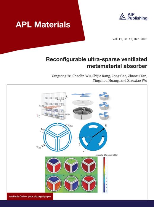
APL Materials
NANOSCIENCE & NANOTECHNOLOGYMATERIALS SCIE-MATERIALS SCIENCE, MULTIDISCIPLINARY
CiteScore
9.60
自引率
3.30%
发文量
199
审稿时长
2 months
期刊介绍:
APL Materials features original, experimental research on significant topical issues within the field of materials science. In order to highlight research at the forefront of materials science, emphasis is given to the quality and timeliness of the work. The journal considers theory or calculation when the work is particularly timely and relevant to applications.
In addition to regular articles, the journal also publishes Special Topics, which report on cutting-edge areas in materials science, such as Perovskite Solar Cells, 2D Materials, and Beyond Lithium Ion Batteries.
 求助内容:
求助内容: 应助结果提醒方式:


