{"title":"A simple, static and stage mounted direct electron detector based electron backscatter diffraction system","authors":"Tianbi Zhang , T. Ben Britton","doi":"10.1016/j.micron.2023.103582","DOIUrl":null,"url":null,"abstract":"<div><p><span><span>To engineer the next generation of advanced materials<span> we must understand their microstructure, and this requires microstructural characterization. This can be achieved through the collection of high contrast, data rich, and insightful microstructural maps. Electron backscatter diffraction (EBSD) has emerged as a popular tool available within the scanning </span></span>electron microscope<span> (SEM), where maps are realized through the repeat capture and analysis of Kikuchi diffraction patterns. Typical commercial EBSD systems require large and sophisticated detectors that are mounted on the side of the SEM vacuum chamber which can be limiting in terms of widespread access to the technique. In this work, we present an alternative open-hardware solution based upon a compact EBSD system with a simple, </span></span>static<span> geometry that uses an off-the-shelf direct electron detector co-mounted with a sample. This simple stage is easy to manufacture and improves our knowledge of the diffraction geometry significantly. Microscope and detector control is achieved through software application programming interface (API) integration. After pattern capture, analysis of the diffraction patterns is performed using open-source analysis within AstroEBSD. To demonstrate the potential of this set up, we present two simple EBSD experiments using a line scan and area mapping. We hope that the present system can inspire simpler EBSD system design for widespread access to the EBSD technique and promote the use of open-source software and hardware in the workflow of EBSD experiments.</span></p></div>","PeriodicalId":18501,"journal":{"name":"Micron","volume":null,"pages":null},"PeriodicalIF":2.5000,"publicationDate":"2023-12-22","publicationTypes":"Journal Article","fieldsOfStudy":null,"isOpenAccess":false,"openAccessPdf":"","citationCount":"0","resultStr":null,"platform":"Semanticscholar","paperid":null,"PeriodicalName":"Micron","FirstCategoryId":"5","ListUrlMain":"https://www.sciencedirect.com/science/article/pii/S0968432823001804","RegionNum":3,"RegionCategory":"工程技术","ArticlePicture":[],"TitleCN":null,"AbstractTextCN":null,"PMCID":null,"EPubDate":"","PubModel":"","JCR":"Q1","JCRName":"MICROSCOPY","Score":null,"Total":0}
引用次数: 0
Abstract
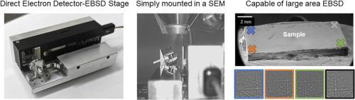
To engineer the next generation of advanced materials we must understand their microstructure, and this requires microstructural characterization. This can be achieved through the collection of high contrast, data rich, and insightful microstructural maps. Electron backscatter diffraction (EBSD) has emerged as a popular tool available within the scanning electron microscope (SEM), where maps are realized through the repeat capture and analysis of Kikuchi diffraction patterns. Typical commercial EBSD systems require large and sophisticated detectors that are mounted on the side of the SEM vacuum chamber which can be limiting in terms of widespread access to the technique. In this work, we present an alternative open-hardware solution based upon a compact EBSD system with a simple, static geometry that uses an off-the-shelf direct electron detector co-mounted with a sample. This simple stage is easy to manufacture and improves our knowledge of the diffraction geometry significantly. Microscope and detector control is achieved through software application programming interface (API) integration. After pattern capture, analysis of the diffraction patterns is performed using open-source analysis within AstroEBSD. To demonstrate the potential of this set up, we present two simple EBSD experiments using a line scan and area mapping. We hope that the present system can inspire simpler EBSD system design for widespread access to the EBSD technique and promote the use of open-source software and hardware in the workflow of EBSD experiments.
期刊介绍:
Micron is an interdisciplinary forum for all work that involves new applications of microscopy or where advanced microscopy plays a central role. The journal will publish on the design, methods, application, practice or theory of microscopy and microanalysis, including reports on optical, electron-beam, X-ray microtomography, and scanning-probe systems. It also aims at the regular publication of review papers, short communications, as well as thematic issues on contemporary developments in microscopy and microanalysis. The journal embraces original research in which microscopy has contributed significantly to knowledge in biology, life science, nanoscience and nanotechnology, materials science and engineering.
 求助内容:
求助内容: 应助结果提醒方式:


