{"title":"Application of intermediate CMOS layer-based defected ground structure to design a dual-band on-chip antenna with improved gain","authors":"Harshavardhan Singh, Sujit Kumar Mandal","doi":"10.1007/s10470-023-02212-5","DOIUrl":null,"url":null,"abstract":"<div><p>In this paper, a novel CPW-fed dual-band on-chip antenna (OCA) by introducing a crossed bowtie shaped defected ground structure (CB-DGS) in one of the intermediate layers of the CMOS layout is proposed. In general, a CPW fed OCA has its ground plane on the same plane containing the antenna. However, in this work, a DGS is introduced in one of the intermediate layer using through silicon vias to obtain dual band characteristics with improved gain performance of the antenna. A 10 dB operating band of 9 GHz (2.25–11.75 GHz) is achieved by employing meandered loop miniaturization technique on the antenna designed on top CMOS layer, wherein the introduction of DGS layer enforced a comparatively less stop band at the middle of the operating band and the resultant structure offered a dual-band resonance characteristic at 3.1 GHz and 10.4 GHz. Here, the intermediate DGS layer between the top-layered antenna and silicon wafer reduces the substrate loss by preventing the coupling of the electromagnetic radiation with the substrate and enhances the antenna gain significantly at both the resonance frequencies respectively by <span>\\(+\\)</span> 16.01 dB and <span>\\(+\\)</span> 12.7 dB. A prototype of the proposed antenna structure is fabricated and the obtained simulated result is validated through experimental measurement.</p></div>","PeriodicalId":7827,"journal":{"name":"Analog Integrated Circuits and Signal Processing","volume":null,"pages":null},"PeriodicalIF":1.2000,"publicationDate":"2023-12-14","publicationTypes":"Journal Article","fieldsOfStudy":null,"isOpenAccess":false,"openAccessPdf":"","citationCount":"0","resultStr":null,"platform":"Semanticscholar","paperid":null,"PeriodicalName":"Analog Integrated Circuits and Signal Processing","FirstCategoryId":"5","ListUrlMain":"https://link.springer.com/article/10.1007/s10470-023-02212-5","RegionNum":4,"RegionCategory":"工程技术","ArticlePicture":[],"TitleCN":null,"AbstractTextCN":null,"PMCID":null,"EPubDate":"","PubModel":"","JCR":"Q4","JCRName":"COMPUTER SCIENCE, HARDWARE & ARCHITECTURE","Score":null,"Total":0}
引用次数: 0
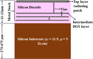
Abstract
In this paper, a novel CPW-fed dual-band on-chip antenna (OCA) by introducing a crossed bowtie shaped defected ground structure (CB-DGS) in one of the intermediate layers of the CMOS layout is proposed. In general, a CPW fed OCA has its ground plane on the same plane containing the antenna. However, in this work, a DGS is introduced in one of the intermediate layer using through silicon vias to obtain dual band characteristics with improved gain performance of the antenna. A 10 dB operating band of 9 GHz (2.25–11.75 GHz) is achieved by employing meandered loop miniaturization technique on the antenna designed on top CMOS layer, wherein the introduction of DGS layer enforced a comparatively less stop band at the middle of the operating band and the resultant structure offered a dual-band resonance characteristic at 3.1 GHz and 10.4 GHz. Here, the intermediate DGS layer between the top-layered antenna and silicon wafer reduces the substrate loss by preventing the coupling of the electromagnetic radiation with the substrate and enhances the antenna gain significantly at both the resonance frequencies respectively by \(+\) 16.01 dB and \(+\) 12.7 dB. A prototype of the proposed antenna structure is fabricated and the obtained simulated result is validated through experimental measurement.
期刊介绍:
Analog Integrated Circuits and Signal Processing is an archival peer reviewed journal dedicated to the design and application of analog, radio frequency (RF), and mixed signal integrated circuits (ICs) as well as signal processing circuits and systems. It features both new research results and tutorial views and reflects the large volume of cutting-edge research activity in the worldwide field today.
A partial list of topics includes analog and mixed signal interface circuits and systems; analog and RFIC design; data converters; active-RC, switched-capacitor, and continuous-time integrated filters; mixed analog/digital VLSI systems; wireless radio transceivers; clock and data recovery circuits; and high speed optoelectronic circuits and systems.

 求助内容:
求助内容: 应助结果提醒方式:


