{"title":"Design and optimization of variable gain LNA for IoT applications using meta-heuristics search algorithms","authors":"Dheeraj Kalra , Mayank Srivastava","doi":"10.1016/j.mee.2023.112125","DOIUrl":null,"url":null,"abstract":"<div><p><span>In this paper, Variable Gain LNA (VG-LNA) parameters are optimized using the Particle Swarm Optimization<span> (PSO), Firefly<span> Algorithm (FA), and Genetic Algorithm (GA). A comparison of the three optimization techniques has been done and FA is depicting better results over GA and PSO. VG-LNA is composed of a Complementary Common Gate (CCG) and Variable Gain Amplifier (VGA). G</span></span></span><sub>m</sub><span><span><span>-boost topology helps in increasing the gain while the current reuse technique provides less </span>power consumption. </span>Optimization algorithms simulated on MATLAB and the result shows minimum Noise Fig. (NF) is 2.62 dB, maximum gain is 17.8 dB, S</span><sub>11</sub><span> i.e. input reflection coefficient is −13.5 dB and S</span><sub>22</sub><span> i.e. output reflection coefficient is −14.7 dB at 50 Ω impedance matching while Figure of Merit1 (FoM1) is 36.14 dB using FA. The FA optimized parameters when simulated on Cadence Virtuoso software using GPDK 45 nm CMOS technology for the frequency range of 26–32 GHz then results show a minimum NF of 2.6 dB at 30.9 GHz, maximum gain of 16.9 dB at 30.5 GHz, S</span><sub>11</sub> is −17.7 dB at 30.5 GHz, S<sub>22</sub> is −21.2 dB at 29 GHz and FoM1 of 34.19 dB. The layout of the realized circuit has an area of 231.695 μm*164.48 μm i.e. 0.03811mm<sup>2</sup>.</p></div>","PeriodicalId":18557,"journal":{"name":"Microelectronic Engineering","volume":null,"pages":null},"PeriodicalIF":2.6000,"publicationDate":"2023-11-28","publicationTypes":"Journal Article","fieldsOfStudy":null,"isOpenAccess":false,"openAccessPdf":"","citationCount":"0","resultStr":null,"platform":"Semanticscholar","paperid":null,"PeriodicalName":"Microelectronic Engineering","FirstCategoryId":"5","ListUrlMain":"https://www.sciencedirect.com/science/article/pii/S0167931723001909","RegionNum":4,"RegionCategory":"工程技术","ArticlePicture":[],"TitleCN":null,"AbstractTextCN":null,"PMCID":null,"EPubDate":"","PubModel":"","JCR":"Q2","JCRName":"ENGINEERING, ELECTRICAL & ELECTRONIC","Score":null,"Total":0}
引用次数: 0
Abstract
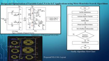
In this paper, Variable Gain LNA (VG-LNA) parameters are optimized using the Particle Swarm Optimization (PSO), Firefly Algorithm (FA), and Genetic Algorithm (GA). A comparison of the three optimization techniques has been done and FA is depicting better results over GA and PSO. VG-LNA is composed of a Complementary Common Gate (CCG) and Variable Gain Amplifier (VGA). Gm-boost topology helps in increasing the gain while the current reuse technique provides less power consumption. Optimization algorithms simulated on MATLAB and the result shows minimum Noise Fig. (NF) is 2.62 dB, maximum gain is 17.8 dB, S11 i.e. input reflection coefficient is −13.5 dB and S22 i.e. output reflection coefficient is −14.7 dB at 50 Ω impedance matching while Figure of Merit1 (FoM1) is 36.14 dB using FA. The FA optimized parameters when simulated on Cadence Virtuoso software using GPDK 45 nm CMOS technology for the frequency range of 26–32 GHz then results show a minimum NF of 2.6 dB at 30.9 GHz, maximum gain of 16.9 dB at 30.5 GHz, S11 is −17.7 dB at 30.5 GHz, S22 is −21.2 dB at 29 GHz and FoM1 of 34.19 dB. The layout of the realized circuit has an area of 231.695 μm*164.48 μm i.e. 0.03811mm2.
期刊介绍:
Microelectronic Engineering is the premier nanoprocessing, and nanotechnology journal focusing on fabrication of electronic, photonic, bioelectronic, electromechanic and fluidic devices and systems, and their applications in the broad areas of electronics, photonics, energy, life sciences, and environment. It covers also the expanding interdisciplinary field of "more than Moore" and "beyond Moore" integrated nanoelectronics / photonics and micro-/nano-/bio-systems. Through its unique mixture of peer-reviewed articles, reviews, accelerated publications, short and Technical notes, and the latest research news on key developments, Microelectronic Engineering provides comprehensive coverage of this exciting, interdisciplinary and dynamic new field for researchers in academia and professionals in industry.

 求助内容:
求助内容: 应助结果提醒方式:


