{"title":"A 2.28mW 100 MS/s 10-bit ping-pong configuration SAR-assisted pipeline ADC","authors":"A. Mosalmani, M. Zahedi Qomi, O. Shoaei","doi":"10.1007/s10470-023-02182-8","DOIUrl":null,"url":null,"abstract":"<div><p>This paper presents a new successive approximation register (SAR)-assisted pipeline analog-to-digital converter (ADC). The coarse stage digital-to-analog converter (DAC) of the proposed ADC is divided into three separate capacitor arrays (a small-DAC and two big-DACs) to increase the sampling rate while simultaneously reducing the power consumption. The small-DAC performs the low-power coarse conversion, and the two big-DACs generate low-noise residue voltage in a ping-pong configuration, reducing the power consumption of the residue amplification. The big-DACs are not involved in the coarse conversion. So, any mismatch between them does not significantly degrade the overall linearity. The unit capacitors of the CDACs are determined according to a comprehensive analysis, including the overall input-referred noise, the bandwidth mismatch, and the static nonlinearity associated with the ping-pong configuration. The proposed ADC is designed and simulated in a 65 nm CMOS technology over process variations. At 1.2 V supply, the ADC achieves a signal-to-noise and distortion ratio (SNDR) of 56.1 dB and a spurious-free dynamic range (SFDR) of 67.3 dB for a Nyquist frequency input sampled at 100 MS/s. The total power consumption is 2.28 mW, resulting in a Walden figure of merit (FoM) of 43 fJ/conversion-step.</p></div>","PeriodicalId":7827,"journal":{"name":"Analog Integrated Circuits and Signal Processing","volume":null,"pages":null},"PeriodicalIF":1.2000,"publicationDate":"2023-11-16","publicationTypes":"Journal Article","fieldsOfStudy":null,"isOpenAccess":false,"openAccessPdf":"","citationCount":"0","resultStr":null,"platform":"Semanticscholar","paperid":null,"PeriodicalName":"Analog Integrated Circuits and Signal Processing","FirstCategoryId":"5","ListUrlMain":"https://link.springer.com/article/10.1007/s10470-023-02182-8","RegionNum":4,"RegionCategory":"工程技术","ArticlePicture":[],"TitleCN":null,"AbstractTextCN":null,"PMCID":null,"EPubDate":"","PubModel":"","JCR":"Q4","JCRName":"COMPUTER SCIENCE, HARDWARE & ARCHITECTURE","Score":null,"Total":0}
引用次数: 0
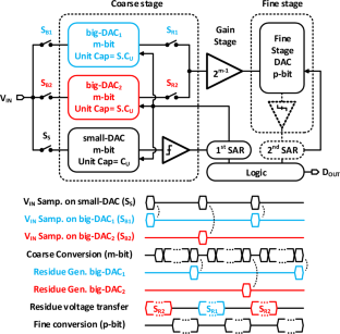
Abstract
This paper presents a new successive approximation register (SAR)-assisted pipeline analog-to-digital converter (ADC). The coarse stage digital-to-analog converter (DAC) of the proposed ADC is divided into three separate capacitor arrays (a small-DAC and two big-DACs) to increase the sampling rate while simultaneously reducing the power consumption. The small-DAC performs the low-power coarse conversion, and the two big-DACs generate low-noise residue voltage in a ping-pong configuration, reducing the power consumption of the residue amplification. The big-DACs are not involved in the coarse conversion. So, any mismatch between them does not significantly degrade the overall linearity. The unit capacitors of the CDACs are determined according to a comprehensive analysis, including the overall input-referred noise, the bandwidth mismatch, and the static nonlinearity associated with the ping-pong configuration. The proposed ADC is designed and simulated in a 65 nm CMOS technology over process variations. At 1.2 V supply, the ADC achieves a signal-to-noise and distortion ratio (SNDR) of 56.1 dB and a spurious-free dynamic range (SFDR) of 67.3 dB for a Nyquist frequency input sampled at 100 MS/s. The total power consumption is 2.28 mW, resulting in a Walden figure of merit (FoM) of 43 fJ/conversion-step.
期刊介绍:
Analog Integrated Circuits and Signal Processing is an archival peer reviewed journal dedicated to the design and application of analog, radio frequency (RF), and mixed signal integrated circuits (ICs) as well as signal processing circuits and systems. It features both new research results and tutorial views and reflects the large volume of cutting-edge research activity in the worldwide field today.
A partial list of topics includes analog and mixed signal interface circuits and systems; analog and RFIC design; data converters; active-RC, switched-capacitor, and continuous-time integrated filters; mixed analog/digital VLSI systems; wireless radio transceivers; clock and data recovery circuits; and high speed optoelectronic circuits and systems.


 求助内容:
求助内容: 应助结果提醒方式:


