{"title":"Area-Selective Deposition: Fundamentals, Applications, and Future Outlook","authors":"Gregory N. Parsons, Robert D. Clark","doi":"10.1021/acs.chemmater.0c00722","DOIUrl":null,"url":null,"abstract":"<p >This review provides an overview of area-selective thin film deposition (ASD) with a primary focus on vapor-phase thin film formation via chemical vapor deposition (CVD) and atomic layer deposition (ALD). Area-selective deposition has been successfully implemented in microelectronic processes, but most approaches to date rely on high-temperature reactions to achieve the desired substrate sensitivity. Continued size and performance scaling of microelectronics, as well as new materials, patterning methods, and device fabrication schemes are seeking solutions for new low-temperature (<400 °C) ASD methods for dielectrics, metals, and organic thin films. To provide an overview of the ASD field, this article critically reviews key challenges that must be overcome for ASD to be successful in microelectronics and other fields, including descriptions of current process application needs. We provide an overview of basic mechanisms in film nucleation during CVD and ALD and summarize current known ASD approaches for semiconductors, metals, dielectrics, and organic materials. For a few key materials, selectivity is quantitatively compared for different reaction precursors, giving important insight into needs for favorable reactant and reaction design. We summarize current limitations of ASD and future opportunities that could be achieved using advanced bottom-up atomic scale processes.</p>","PeriodicalId":33,"journal":{"name":"Chemistry of Materials","volume":"32 12","pages":"4920–4953"},"PeriodicalIF":7.2000,"publicationDate":"2020-05-14","publicationTypes":"Journal Article","fieldsOfStudy":null,"isOpenAccess":false,"openAccessPdf":"https://sci-hub-pdf.com/10.1021/acs.chemmater.0c00722","citationCount":"123","resultStr":null,"platform":"Semanticscholar","paperid":null,"PeriodicalName":"Chemistry of Materials","FirstCategoryId":"88","ListUrlMain":"https://pubs.acs.org/doi/10.1021/acs.chemmater.0c00722","RegionNum":2,"RegionCategory":"材料科学","ArticlePicture":[],"TitleCN":null,"AbstractTextCN":null,"PMCID":null,"EPubDate":"","PubModel":"","JCR":"Q2","JCRName":"CHEMISTRY, PHYSICAL","Score":null,"Total":0}
引用次数: 123
Abstract
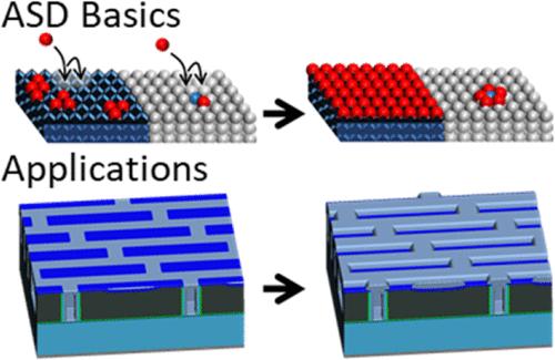
This review provides an overview of area-selective thin film deposition (ASD) with a primary focus on vapor-phase thin film formation via chemical vapor deposition (CVD) and atomic layer deposition (ALD). Area-selective deposition has been successfully implemented in microelectronic processes, but most approaches to date rely on high-temperature reactions to achieve the desired substrate sensitivity. Continued size and performance scaling of microelectronics, as well as new materials, patterning methods, and device fabrication schemes are seeking solutions for new low-temperature (<400 °C) ASD methods for dielectrics, metals, and organic thin films. To provide an overview of the ASD field, this article critically reviews key challenges that must be overcome for ASD to be successful in microelectronics and other fields, including descriptions of current process application needs. We provide an overview of basic mechanisms in film nucleation during CVD and ALD and summarize current known ASD approaches for semiconductors, metals, dielectrics, and organic materials. For a few key materials, selectivity is quantitatively compared for different reaction precursors, giving important insight into needs for favorable reactant and reaction design. We summarize current limitations of ASD and future opportunities that could be achieved using advanced bottom-up atomic scale processes.
期刊介绍:
The journal Chemistry of Materials focuses on publishing original research at the intersection of materials science and chemistry. The studies published in the journal involve chemistry as a prominent component and explore topics such as the design, synthesis, characterization, processing, understanding, and application of functional or potentially functional materials. The journal covers various areas of interest, including inorganic and organic solid-state chemistry, nanomaterials, biomaterials, thin films and polymers, and composite/hybrid materials. The journal particularly seeks papers that highlight the creation or development of innovative materials with novel optical, electrical, magnetic, catalytic, or mechanical properties. It is essential that manuscripts on these topics have a primary focus on the chemistry of materials and represent a significant advancement compared to prior research. Before external reviews are sought, submitted manuscripts undergo a review process by a minimum of two editors to ensure their appropriateness for the journal and the presence of sufficient evidence of a significant advance that will be of broad interest to the materials chemistry community.
 求助内容:
求助内容: 应助结果提醒方式:


