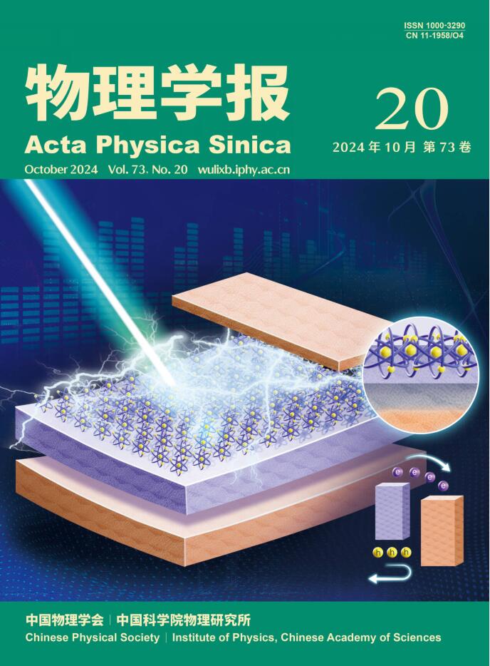
{"title":"非载流子注入LED的载流子输运模型","authors":"Zhao Jian-Cheng, Wu Chao-Xing, Guo Tai-Liang","doi":"10.7498/aps.72.20221831","DOIUrl":null,"url":null,"abstract":"Non-carrier-injection light-emitting diodes (NCI-LEDs) are expected to be widely used in next generation micro-display technologies, including Micro-LEDs and nano-pixel light-emitting displays due to their simple device structure. However, because there is no charge carrier injection from external electrodes, carrier transport behavior of the NCI-LED cannot be described by using the traditional PN junction and LED theory. Therefore, establishing a carrier-transport model for the NCI-LED is of great significance for understanding its working mechanism and for improving device performance. In this paper, carrier transport mathematical model of the NCI-LED is established and the mechanical behavior of charge-carrier transport is analyzed quantitatively. Based on the mathematical model, the working mechanism of the NCI-LED is explained, the carrier transport characteristics of the device are obtained. Additionally, the key features, including the length of the induced charge region, the forward biased voltage across the internal PN junction, and the reverse biased voltage across the internal PN junction are studied. Their relationships with the applied frequency of the applied driving voltage are revealed. It is found that both the forward and reverse biases of the internal PN junction increase with the driving frequency. When the driving frequency reaches a certain value, the forward and reverse bias of the PN junction would be maintained at a maximum value. Moreover, the length of the induced charge region decreases with the increase of the driving frequency, and when the frequency reaches a certain value, the induced charge region would always be in the state of exhaustion. According to the mathematical model, suggestions for the device optimization design are provided: (1) Reducing the doping concentration of the induced charge regions can effectively increase the voltage drop across the internal LED; (2) Employing the tunneling effect occurring in the reverse-biased PN junction can effectively improve the electroluminescence intensity; (3) Using square-wave driving voltage can obtain a larger voltage drop across the internal LED and increase the electroluminescence intensity. This work on the carrier transport model is expected to provide a clear physical image for understanding the working mechanism of NCI-LED, and to provide a theoretical guidance for optimizing the device structure.","PeriodicalId":6995,"journal":{"name":"物理学报","volume":"20 1","pages":""},"PeriodicalIF":0.8000,"publicationDate":"2023-01-01","publicationTypes":"Journal Article","fieldsOfStudy":null,"isOpenAccess":false,"openAccessPdf":"","citationCount":"0","resultStr":"{\"title\":\"Carrier Transport Model of Non-carrier-injection LED\",\"authors\":\"Zhao Jian-Cheng, Wu Chao-Xing, Guo Tai-Liang\",\"doi\":\"10.7498/aps.72.20221831\",\"DOIUrl\":null,\"url\":null,\"abstract\":\"Non-carrier-injection light-emitting diodes (NCI-LEDs) are expected to be widely used in next generation micro-display technologies, including Micro-LEDs and nano-pixel light-emitting displays due to their simple device structure. However, because there is no charge carrier injection from external electrodes, carrier transport behavior of the NCI-LED cannot be described by using the traditional PN junction and LED theory. Therefore, establishing a carrier-transport model for the NCI-LED is of great significance for understanding its working mechanism and for improving device performance. In this paper, carrier transport mathematical model of the NCI-LED is established and the mechanical behavior of charge-carrier transport is analyzed quantitatively. Based on the mathematical model, the working mechanism of the NCI-LED is explained, the carrier transport characteristics of the device are obtained. Additionally, the key features, including the length of the induced charge region, the forward biased voltage across the internal PN junction, and the reverse biased voltage across the internal PN junction are studied. Their relationships with the applied frequency of the applied driving voltage are revealed. It is found that both the forward and reverse biases of the internal PN junction increase with the driving frequency. When the driving frequency reaches a certain value, the forward and reverse bias of the PN junction would be maintained at a maximum value. Moreover, the length of the induced charge region decreases with the increase of the driving frequency, and when the frequency reaches a certain value, the induced charge region would always be in the state of exhaustion. According to the mathematical model, suggestions for the device optimization design are provided: (1) Reducing the doping concentration of the induced charge regions can effectively increase the voltage drop across the internal LED; (2) Employing the tunneling effect occurring in the reverse-biased PN junction can effectively improve the electroluminescence intensity; (3) Using square-wave driving voltage can obtain a larger voltage drop across the internal LED and increase the electroluminescence intensity. This work on the carrier transport model is expected to provide a clear physical image for understanding the working mechanism of NCI-LED, and to provide a theoretical guidance for optimizing the device structure.\",\"PeriodicalId\":6995,\"journal\":{\"name\":\"物理学报\",\"volume\":\"20 1\",\"pages\":\"\"},\"PeriodicalIF\":0.8000,\"publicationDate\":\"2023-01-01\",\"publicationTypes\":\"Journal Article\",\"fieldsOfStudy\":null,\"isOpenAccess\":false,\"openAccessPdf\":\"\",\"citationCount\":\"0\",\"resultStr\":null,\"platform\":\"Semanticscholar\",\"paperid\":null,\"PeriodicalName\":\"物理学报\",\"FirstCategoryId\":\"101\",\"ListUrlMain\":\"https://doi.org/10.7498/aps.72.20221831\",\"RegionNum\":4,\"RegionCategory\":\"物理与天体物理\",\"ArticlePicture\":[],\"TitleCN\":null,\"AbstractTextCN\":null,\"PMCID\":null,\"EPubDate\":\"\",\"PubModel\":\"\",\"JCR\":\"Q3\",\"JCRName\":\"PHYSICS, MULTIDISCIPLINARY\",\"Score\":null,\"Total\":0}","platform":"Semanticscholar","paperid":null,"PeriodicalName":"物理学报","FirstCategoryId":"101","ListUrlMain":"https://doi.org/10.7498/aps.72.20221831","RegionNum":4,"RegionCategory":"物理与天体物理","ArticlePicture":[],"TitleCN":null,"AbstractTextCN":null,"PMCID":null,"EPubDate":"","PubModel":"","JCR":"Q3","JCRName":"PHYSICS, MULTIDISCIPLINARY","Score":null,"Total":0}
Carrier Transport Model of Non-carrier-injection LED
Non-carrier-injection light-emitting diodes (NCI-LEDs) are expected to be widely used in next generation micro-display technologies, including Micro-LEDs and nano-pixel light-emitting displays due to their simple device structure. However, because there is no charge carrier injection from external electrodes, carrier transport behavior of the NCI-LED cannot be described by using the traditional PN junction and LED theory. Therefore, establishing a carrier-transport model for the NCI-LED is of great significance for understanding its working mechanism and for improving device performance. In this paper, carrier transport mathematical model of the NCI-LED is established and the mechanical behavior of charge-carrier transport is analyzed quantitatively. Based on the mathematical model, the working mechanism of the NCI-LED is explained, the carrier transport characteristics of the device are obtained. Additionally, the key features, including the length of the induced charge region, the forward biased voltage across the internal PN junction, and the reverse biased voltage across the internal PN junction are studied. Their relationships with the applied frequency of the applied driving voltage are revealed. It is found that both the forward and reverse biases of the internal PN junction increase with the driving frequency. When the driving frequency reaches a certain value, the forward and reverse bias of the PN junction would be maintained at a maximum value. Moreover, the length of the induced charge region decreases with the increase of the driving frequency, and when the frequency reaches a certain value, the induced charge region would always be in the state of exhaustion. According to the mathematical model, suggestions for the device optimization design are provided: (1) Reducing the doping concentration of the induced charge regions can effectively increase the voltage drop across the internal LED; (2) Employing the tunneling effect occurring in the reverse-biased PN junction can effectively improve the electroluminescence intensity; (3) Using square-wave driving voltage can obtain a larger voltage drop across the internal LED and increase the electroluminescence intensity. This work on the carrier transport model is expected to provide a clear physical image for understanding the working mechanism of NCI-LED, and to provide a theoretical guidance for optimizing the device structure.
期刊介绍:
Acta Physica Sinica (Acta Phys. Sin.) is supervised by Chinese Academy of Sciences and sponsored by Chinese Physical Society and Institute of Physics, Chinese Academy of Sciences. Published by Chinese Physical Society and launched in 1933, it is a semimonthly journal with about 40 articles per issue.
It publishes original and top quality research papers, rapid communications and reviews in all branches of physics in Chinese. Acta Phys. Sin. enjoys high reputation among Chinese physics journals and plays a key role in bridging China and rest of the world in physics research. Specific areas of interest include: Condensed matter and materials physics; Atomic, molecular, and optical physics; Statistical, nonlinear, and soft matter physics; Plasma physics; Interdisciplinary physics.