MoS2/MoTe2垂直异质结的电荷传输及其调制

IF 0.8 4区 物理与天体物理 Q3 PHYSICS, MULTIDISCIPLINARY
Heng-Di Wen, Yue Liu, Liang Zhen, Yang Li, Cheng-Yan Xu
{"title":"MoS2/MoTe2垂直异质结的电荷传输及其调制","authors":"Heng-Di Wen, Yue Liu, Liang Zhen, Yang Li, Cheng-Yan Xu","doi":"10.7498/aps.72.20221768","DOIUrl":null,"url":null,"abstract":"Two-dimensional material heterojunction device with unique photoelectric properties due to its nanoscale thickness and van der Waals contact surface. In this paper, a MoS2/MoTe2 vertical vdWs heterojunction device with Gate-tunable is constructed. The Kelvin probe force microscopy (KPFM) technology is combined with the electric transport measurement technology, which reveals the charge transport behavior of the MoS2/MoTe2 heterojunction under dark and light conditions, including the bipolarity characteristics of the transition from n-n+ junction to p-n junction. This paper comprehensively and systematically explains the charge transport mechanism of heterojunction, including the charge transmission process of n-n+ junction and p-n junction under positive and negative bias conditions, the transformation of nodule behavior with gate voltage, the influence of barriers on charge transmission, the different rectification characteristics between n-n+ junction and p-n junction, the major role of source and leakage bias voltage on band tunneling, and the influence of photogenerated carriers on electrical transmission. The method in this paper can be generalized to other two-dimensional heterojunction systems and provides an important reference and reference for improving the performance of two-dimensional semiconductor devices and their applications in the future.","PeriodicalId":6995,"journal":{"name":"物理学报","volume":"59 1","pages":""},"PeriodicalIF":0.8000,"publicationDate":"2023-01-01","publicationTypes":"Journal Article","fieldsOfStudy":null,"isOpenAccess":false,"openAccessPdf":"","citationCount":"0","resultStr":"{\"title\":\"Charge transmission of MoS2/MoTe2 vertical heterojunction and it's modulation\",\"authors\":\"Heng-Di Wen, Yue Liu, Liang Zhen, Yang Li, Cheng-Yan Xu\",\"doi\":\"10.7498/aps.72.20221768\",\"DOIUrl\":null,\"url\":null,\"abstract\":\"Two-dimensional material heterojunction device with unique photoelectric properties due to its nanoscale thickness and van der Waals contact surface. In this paper, a MoS2/MoTe2 vertical vdWs heterojunction device with Gate-tunable is constructed. The Kelvin probe force microscopy (KPFM) technology is combined with the electric transport measurement technology, which reveals the charge transport behavior of the MoS2/MoTe2 heterojunction under dark and light conditions, including the bipolarity characteristics of the transition from n-n+ junction to p-n junction. This paper comprehensively and systematically explains the charge transport mechanism of heterojunction, including the charge transmission process of n-n+ junction and p-n junction under positive and negative bias conditions, the transformation of nodule behavior with gate voltage, the influence of barriers on charge transmission, the different rectification characteristics between n-n+ junction and p-n junction, the major role of source and leakage bias voltage on band tunneling, and the influence of photogenerated carriers on electrical transmission. The method in this paper can be generalized to other two-dimensional heterojunction systems and provides an important reference and reference for improving the performance of two-dimensional semiconductor devices and their applications in the future.\",\"PeriodicalId\":6995,\"journal\":{\"name\":\"物理学报\",\"volume\":\"59 1\",\"pages\":\"\"},\"PeriodicalIF\":0.8000,\"publicationDate\":\"2023-01-01\",\"publicationTypes\":\"Journal Article\",\"fieldsOfStudy\":null,\"isOpenAccess\":false,\"openAccessPdf\":\"\",\"citationCount\":\"0\",\"resultStr\":null,\"platform\":\"Semanticscholar\",\"paperid\":null,\"PeriodicalName\":\"物理学报\",\"FirstCategoryId\":\"101\",\"ListUrlMain\":\"https://doi.org/10.7498/aps.72.20221768\",\"RegionNum\":4,\"RegionCategory\":\"物理与天体物理\",\"ArticlePicture\":[],\"TitleCN\":null,\"AbstractTextCN\":null,\"PMCID\":null,\"EPubDate\":\"\",\"PubModel\":\"\",\"JCR\":\"Q3\",\"JCRName\":\"PHYSICS, MULTIDISCIPLINARY\",\"Score\":null,\"Total\":0}","platform":"Semanticscholar","paperid":null,"PeriodicalName":"物理学报","FirstCategoryId":"101","ListUrlMain":"https://doi.org/10.7498/aps.72.20221768","RegionNum":4,"RegionCategory":"物理与天体物理","ArticlePicture":[],"TitleCN":null,"AbstractTextCN":null,"PMCID":null,"EPubDate":"","PubModel":"","JCR":"Q3","JCRName":"PHYSICS, MULTIDISCIPLINARY","Score":null,"Total":0}
引用次数: 0

摘要

二维材料异质结器件由于其纳米级厚度和范德华接触面而具有独特的光电性能。本文构造了一个栅极可调谐的MoS2/MoTe2垂直vdWs异质结器件。将开尔文探针力显微镜(KPFM)技术与电输运测量技术相结合,揭示了MoS2/MoTe2异质结在黑暗和光照条件下的电荷输运行为,包括从n-n+结向p-n结转变的双极性特征。本文全面系统地阐述了异质结的电荷输运机理,包括正负偏置条件下n-n+结和p-n结的电荷输运过程、栅极电压对结行为的改变、势垒对电荷输运的影响、n-n+结和p-n结的不同整流特性、源偏压和漏偏压对带隧穿的主要作用。以及光生载流子对电传输的影响。本文的方法可以推广到其他二维异质结系统,为今后提高二维半导体器件的性能及其应用提供了重要的参考和参考。
本文章由计算机程序翻译,如有差异,请以英文原文为准。
Charge transmission of MoS2/MoTe2 vertical heterojunction and it's modulation
Two-dimensional material heterojunction device with unique photoelectric properties due to its nanoscale thickness and van der Waals contact surface. In this paper, a MoS2/MoTe2 vertical vdWs heterojunction device with Gate-tunable is constructed. The Kelvin probe force microscopy (KPFM) technology is combined with the electric transport measurement technology, which reveals the charge transport behavior of the MoS2/MoTe2 heterojunction under dark and light conditions, including the bipolarity characteristics of the transition from n-n+ junction to p-n junction. This paper comprehensively and systematically explains the charge transport mechanism of heterojunction, including the charge transmission process of n-n+ junction and p-n junction under positive and negative bias conditions, the transformation of nodule behavior with gate voltage, the influence of barriers on charge transmission, the different rectification characteristics between n-n+ junction and p-n junction, the major role of source and leakage bias voltage on band tunneling, and the influence of photogenerated carriers on electrical transmission. The method in this paper can be generalized to other two-dimensional heterojunction systems and provides an important reference and reference for improving the performance of two-dimensional semiconductor devices and their applications in the future.
求助全文
通过发布文献求助,成功后即可免费获取论文全文。 去求助
来源期刊
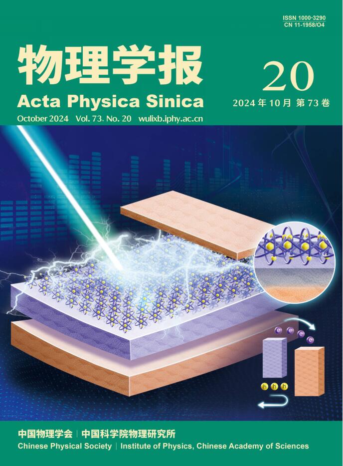
物理学报
物理学报 物理-物理:综合
CiteScore
1.70
自引率
30.00%
发文量
31245
审稿时长
1.9 months
期刊介绍: Acta Physica Sinica (Acta Phys. Sin.) is supervised by Chinese Academy of Sciences and sponsored by Chinese Physical Society and Institute of Physics, Chinese Academy of Sciences. Published by Chinese Physical Society and launched in 1933, it is a semimonthly journal with about 40 articles per issue. It publishes original and top quality research papers, rapid communications and reviews in all branches of physics in Chinese. Acta Phys. Sin. enjoys high reputation among Chinese physics journals and plays a key role in bridging China and rest of the world in physics research. Specific areas of interest include: Condensed matter and materials physics; Atomic, molecular, and optical physics; Statistical, nonlinear, and soft matter physics; Plasma physics; Interdisciplinary physics.
×
引用
GB/T 7714-2015
复制
MLA
复制
APA
复制
导出至
BibTeX EndNote RefMan NoteFirst NoteExpress
×
提示
您的信息不完整,为了账户安全,请先补充。
现在去补充
×
提示
您因"违规操作"
具体请查看互助需知
我知道了
×
提示
确定
请完成安全验证×
copy
已复制链接
快去分享给好友吧!
我知道了
右上角分享
点击右上角分享
0
联系我们:info@booksci.cn Book学术提供免费学术资源搜索服务,方便国内外学者检索中英文文献。致力于提供最便捷和优质的服务体验。 Copyright © 2023 布克学术 All rights reserved.
京ICP备2023020795号-1
ghs 京公网安备 11010802042870号
Book学术文献互助
Book学术文献互助群
群 号:481959085
Book学术官方微信