D. M. Lebedev, S. A. Nefedov, D. A. Shishkina, I. A. Shishkin, V. I. Chepurnov, V. V. Taneev
{"title":"HTCVD法制备3C SiC/Si薄膜的生长特性","authors":"D. M. Lebedev, S. A. Nefedov, D. A. Shishkina, I. A. Shishkin, V. I. Chepurnov, V. V. Taneev","doi":"10.3103/S1060992X23050132","DOIUrl":null,"url":null,"abstract":"<p>This work is devoted to the study of the morphology and structure of 3C-SiC/Si films obtained by the high-temperature chemical vapor deposition (HT CVD) method. Epitaxial growth is achieved by transforming the crystal by coordinated substitution of atoms, in which the overall structure of bonds between atoms is not destroyed. At the first stage of the conversion, the first half of silicon atoms Si is successively replaced by carbon atoms C as a result of reaction of Si with gas CO, and an epitaxial layer of cubic silicon carbide SiC-3C is obtained. At the second stage, the remaining half of Si atoms is consistently replaced by C atoms due to the reaction of SiC with CF4 gas. Depending on the orientation of the silicon surface, the pressure of the reagent gas, the temperature and time of growth, carbon structures with various properties are obtained, from nanodiamonds to nanotubes and onion carbon. The key feature of this method is that the substrate orders the resulting structures using the initial chemical bonds between atoms in silicon. Photographs of the surface of the structures are presented, demonstrating the features of silicon carbide film growth at different levels of the substrate holder. Analysis of rotational X-ray diffraction patterns showed the presence of silicon carbide films of the 3-C polytype.</p>","PeriodicalId":721,"journal":{"name":"Optical Memory and Neural Networks","volume":null,"pages":null},"PeriodicalIF":1.0000,"publicationDate":"2023-11-03","publicationTypes":"Journal Article","fieldsOfStudy":null,"isOpenAccess":false,"openAccessPdf":"","citationCount":"0","resultStr":"{\"title\":\"Growth Features of 3C-SiC/Si Films Fabricated by HTCVD\",\"authors\":\"D. M. Lebedev, S. A. Nefedov, D. A. Shishkina, I. A. Shishkin, V. I. Chepurnov, V. V. Taneev\",\"doi\":\"10.3103/S1060992X23050132\",\"DOIUrl\":null,\"url\":null,\"abstract\":\"<p>This work is devoted to the study of the morphology and structure of 3C-SiC/Si films obtained by the high-temperature chemical vapor deposition (HT CVD) method. Epitaxial growth is achieved by transforming the crystal by coordinated substitution of atoms, in which the overall structure of bonds between atoms is not destroyed. At the first stage of the conversion, the first half of silicon atoms Si is successively replaced by carbon atoms C as a result of reaction of Si with gas CO, and an epitaxial layer of cubic silicon carbide SiC-3C is obtained. At the second stage, the remaining half of Si atoms is consistently replaced by C atoms due to the reaction of SiC with CF4 gas. Depending on the orientation of the silicon surface, the pressure of the reagent gas, the temperature and time of growth, carbon structures with various properties are obtained, from nanodiamonds to nanotubes and onion carbon. The key feature of this method is that the substrate orders the resulting structures using the initial chemical bonds between atoms in silicon. Photographs of the surface of the structures are presented, demonstrating the features of silicon carbide film growth at different levels of the substrate holder. Analysis of rotational X-ray diffraction patterns showed the presence of silicon carbide films of the 3-C polytype.</p>\",\"PeriodicalId\":721,\"journal\":{\"name\":\"Optical Memory and Neural Networks\",\"volume\":null,\"pages\":null},\"PeriodicalIF\":1.0000,\"publicationDate\":\"2023-11-03\",\"publicationTypes\":\"Journal Article\",\"fieldsOfStudy\":null,\"isOpenAccess\":false,\"openAccessPdf\":\"\",\"citationCount\":\"0\",\"resultStr\":null,\"platform\":\"Semanticscholar\",\"paperid\":null,\"PeriodicalName\":\"Optical Memory and Neural Networks\",\"FirstCategoryId\":\"1085\",\"ListUrlMain\":\"https://link.springer.com/article/10.3103/S1060992X23050132\",\"RegionNum\":0,\"RegionCategory\":null,\"ArticlePicture\":[],\"TitleCN\":null,\"AbstractTextCN\":null,\"PMCID\":null,\"EPubDate\":\"\",\"PubModel\":\"\",\"JCR\":\"Q4\",\"JCRName\":\"OPTICS\",\"Score\":null,\"Total\":0}","platform":"Semanticscholar","paperid":null,"PeriodicalName":"Optical Memory and Neural Networks","FirstCategoryId":"1085","ListUrlMain":"https://link.springer.com/article/10.3103/S1060992X23050132","RegionNum":0,"RegionCategory":null,"ArticlePicture":[],"TitleCN":null,"AbstractTextCN":null,"PMCID":null,"EPubDate":"","PubModel":"","JCR":"Q4","JCRName":"OPTICS","Score":null,"Total":0}
Growth Features of 3C-SiC/Si Films Fabricated by HTCVD
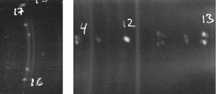
This work is devoted to the study of the morphology and structure of 3C-SiC/Si films obtained by the high-temperature chemical vapor deposition (HT CVD) method. Epitaxial growth is achieved by transforming the crystal by coordinated substitution of atoms, in which the overall structure of bonds between atoms is not destroyed. At the first stage of the conversion, the first half of silicon atoms Si is successively replaced by carbon atoms C as a result of reaction of Si with gas CO, and an epitaxial layer of cubic silicon carbide SiC-3C is obtained. At the second stage, the remaining half of Si atoms is consistently replaced by C atoms due to the reaction of SiC with CF4 gas. Depending on the orientation of the silicon surface, the pressure of the reagent gas, the temperature and time of growth, carbon structures with various properties are obtained, from nanodiamonds to nanotubes and onion carbon. The key feature of this method is that the substrate orders the resulting structures using the initial chemical bonds between atoms in silicon. Photographs of the surface of the structures are presented, demonstrating the features of silicon carbide film growth at different levels of the substrate holder. Analysis of rotational X-ray diffraction patterns showed the presence of silicon carbide films of the 3-C polytype.
期刊介绍:
The journal covers a wide range of issues in information optics such as optical memory, mechanisms for optical data recording and processing, photosensitive materials, optical, optoelectronic and holographic nanostructures, and many other related topics. Papers on memory systems using holographic and biological structures and concepts of brain operation are also included. The journal pays particular attention to research in the field of neural net systems that may lead to a new generation of computional technologies by endowing them with intelligence.
 求助内容:
求助内容: 应助结果提醒方式:


