Peixin Chen, Wei Shen, Zhiqin Chen, Chongyang Li, Silin Han, Yunwen Wu, Tao Hang, Ming Li
{"title":"直流电沉积中纳米孪晶铜的表面原子迁移与二维成核生长","authors":"Peixin Chen, Wei Shen, Zhiqin Chen, Chongyang Li, Silin Han, Yunwen Wu, Tao Hang, Ming Li","doi":"10.1016/j.actamat.2023.119468","DOIUrl":null,"url":null,"abstract":"<div><p>Direct-current (DC) Electrodeposited nanotwinned copper (nt-Cu) is a promising candidate for interconnection materials in integrated circuit for its excellent mechanical, electrical and thermal properties. However, the formation mechanism of nanotwins during DC electrodeposition<span> of nt-Cu remains unclear. In this study, a two-dimensional nucleation and growth model of nt-Cu is established. The critical nucleation size and average twin spacing were evaluated theoretically. The results demonstrate a relatively high probability of twin nucleation through random stacking with the average twin spacing derived to be only ∼1 nm. The gap between theoretical and observed twinning probability can be ascribed to the surface migration-induced dissipation of nuclei. Molecular dynamics simulation further confirms the formation and subsequent dissipation of nuclei during deposition of Cu. By providing a clear illustration of nanotwin formation process, this study contributes to the understanding of nt-Cu electrodeposition.</span></p></div>","PeriodicalId":238,"journal":{"name":"Acta Materialia","volume":"262 ","pages":"Article 119468"},"PeriodicalIF":8.3000,"publicationDate":"2023-10-28","publicationTypes":"Journal Article","fieldsOfStudy":null,"isOpenAccess":false,"openAccessPdf":"","citationCount":"0","resultStr":"{\"title\":\"Surface atom migration-involved two-dimensional nucleation and growth of nanotwinned copper in DC electrodeposition\",\"authors\":\"Peixin Chen, Wei Shen, Zhiqin Chen, Chongyang Li, Silin Han, Yunwen Wu, Tao Hang, Ming Li\",\"doi\":\"10.1016/j.actamat.2023.119468\",\"DOIUrl\":null,\"url\":null,\"abstract\":\"<div><p>Direct-current (DC) Electrodeposited nanotwinned copper (nt-Cu) is a promising candidate for interconnection materials in integrated circuit for its excellent mechanical, electrical and thermal properties. However, the formation mechanism of nanotwins during DC electrodeposition<span> of nt-Cu remains unclear. In this study, a two-dimensional nucleation and growth model of nt-Cu is established. The critical nucleation size and average twin spacing were evaluated theoretically. The results demonstrate a relatively high probability of twin nucleation through random stacking with the average twin spacing derived to be only ∼1 nm. The gap between theoretical and observed twinning probability can be ascribed to the surface migration-induced dissipation of nuclei. Molecular dynamics simulation further confirms the formation and subsequent dissipation of nuclei during deposition of Cu. By providing a clear illustration of nanotwin formation process, this study contributes to the understanding of nt-Cu electrodeposition.</span></p></div>\",\"PeriodicalId\":238,\"journal\":{\"name\":\"Acta Materialia\",\"volume\":\"262 \",\"pages\":\"Article 119468\"},\"PeriodicalIF\":8.3000,\"publicationDate\":\"2023-10-28\",\"publicationTypes\":\"Journal Article\",\"fieldsOfStudy\":null,\"isOpenAccess\":false,\"openAccessPdf\":\"\",\"citationCount\":\"0\",\"resultStr\":null,\"platform\":\"Semanticscholar\",\"paperid\":null,\"PeriodicalName\":\"Acta Materialia\",\"FirstCategoryId\":\"88\",\"ListUrlMain\":\"https://www.sciencedirect.com/science/article/pii/S1359645423007978\",\"RegionNum\":1,\"RegionCategory\":\"材料科学\",\"ArticlePicture\":[],\"TitleCN\":null,\"AbstractTextCN\":null,\"PMCID\":null,\"EPubDate\":\"\",\"PubModel\":\"\",\"JCR\":\"Q1\",\"JCRName\":\"MATERIALS SCIENCE, MULTIDISCIPLINARY\",\"Score\":null,\"Total\":0}","platform":"Semanticscholar","paperid":null,"PeriodicalName":"Acta Materialia","FirstCategoryId":"88","ListUrlMain":"https://www.sciencedirect.com/science/article/pii/S1359645423007978","RegionNum":1,"RegionCategory":"材料科学","ArticlePicture":[],"TitleCN":null,"AbstractTextCN":null,"PMCID":null,"EPubDate":"","PubModel":"","JCR":"Q1","JCRName":"MATERIALS SCIENCE, MULTIDISCIPLINARY","Score":null,"Total":0}
Surface atom migration-involved two-dimensional nucleation and growth of nanotwinned copper in DC electrodeposition
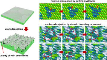
Direct-current (DC) Electrodeposited nanotwinned copper (nt-Cu) is a promising candidate for interconnection materials in integrated circuit for its excellent mechanical, electrical and thermal properties. However, the formation mechanism of nanotwins during DC electrodeposition of nt-Cu remains unclear. In this study, a two-dimensional nucleation and growth model of nt-Cu is established. The critical nucleation size and average twin spacing were evaluated theoretically. The results demonstrate a relatively high probability of twin nucleation through random stacking with the average twin spacing derived to be only ∼1 nm. The gap between theoretical and observed twinning probability can be ascribed to the surface migration-induced dissipation of nuclei. Molecular dynamics simulation further confirms the formation and subsequent dissipation of nuclei during deposition of Cu. By providing a clear illustration of nanotwin formation process, this study contributes to the understanding of nt-Cu electrodeposition.
期刊介绍:
Acta Materialia serves as a platform for publishing full-length, original papers and commissioned overviews that contribute to a profound understanding of the correlation between the processing, structure, and properties of inorganic materials. The journal seeks papers with high impact potential or those that significantly propel the field forward. The scope includes the atomic and molecular arrangements, chemical and electronic structures, and microstructure of materials, focusing on their mechanical or functional behavior across all length scales, including nanostructures.
 求助内容:
求助内容: 应助结果提醒方式:


