通过高分辨率静电门控实现VO_ 2金属-绝缘体跃迁的零维

IF 8.6 2区 材料科学 Q1 MATERIALS SCIENCE, MULTIDISCIPLINARY
Takeaki Yajima, Yusuke Samata, Satoshi Hamasuna, Satya Prakash Pati, Akira Toriumi
{"title":"通过高分辨率静电门控实现VO_ 2金属-绝缘体跃迁的零维","authors":"Takeaki Yajima, Yusuke Samata, Satoshi Hamasuna, Satya Prakash Pati, Akira Toriumi","doi":"10.1038/s41427-023-00486-9","DOIUrl":null,"url":null,"abstract":"An understanding of the phase transitions at the nanoscale is essential in state-of-the-art engineering1–5, instead of simply averaging the heterogeneous domains formed during phase transitions6,7. However, as materials are scaled down, the steepness of the phase transition rapidly increases8–13 and requires extremely high precision in the control method. Here, a three-terminal device, which could precisely control the phase transition electrically14–19, was applied for the first time to a scaled-down metal-insulator transition material VO2. The crossover from continuous to binary transitions with the scaled-down material was clarified, and the critical channel length was successfully elucidated via phase boundary energy. Notably, below the critical channel length, the spatial degrees of freedom degenerated, and the impact of drain voltage application disappeared in the phase transition, indicating zero-dimensionality of the VO2 channel. This zero-dimensionality could be the fundamental property in the scaled-down phase transition and have a significant impact on various fields that need nanoscale engineering. Controlling the atomic configuration of nanoscale devices to alter their electrical properties has been demonstrated by scientists in Japan. The crystalline structure of a solid can switch between atomic arrangements, or phases, with a change in temperature or electric field. Devices that control these phase transitions have potential applications as computer memories or sensors but such control becomes more difficult as the device gets smaller. Takeaki Yajima from Kyusyu University, Fukuoka, and colleagues have demonstrated the electrically induced change from a metallic to an insulating phase in long, thin, submicrometer vanadium dioxide devices. The team showed that while longer devices exhibited a continuous transition between the two phases as a voltage was applied, the submicrometer devices unexpectedly showed a completely binary switching behavior. Knowing about this different behavior will aid the engineering of nanoscale electronic devices. Although the electrostatic tuning by three-terminal devices is generally weak for phase transition materials, it can control phases with much hither precision than temperature or pressure. This technique was applied to the scaled-down VO2 metal-insulator transitions, where the material phase is controlled by the gate voltage. The crossover from continuous to binary transition with scaling down was demonstrated, and the critical channel length was given by domain boundary instability. Interestingly, below the critical channel length, the influence of the noncritical stimulus (drain voltage in this case) disappeared because the spatial degree of freedom is lost in the single-domain VO2 channel.","PeriodicalId":19382,"journal":{"name":"Npg Asia Materials","volume":"15 1","pages":"1-6"},"PeriodicalIF":8.6000,"publicationDate":"2023-06-30","publicationTypes":"Journal Article","fieldsOfStudy":null,"isOpenAccess":false,"openAccessPdf":"https://www.nature.com/articles/s41427-023-00486-9.pdf","citationCount":"0","resultStr":"{\"title\":\"Zero-dimensionality of a scaled-down VO2 metal-insulator transition via high-resolution electrostatic gating\",\"authors\":\"Takeaki Yajima, Yusuke Samata, Satoshi Hamasuna, Satya Prakash Pati, Akira Toriumi\",\"doi\":\"10.1038/s41427-023-00486-9\",\"DOIUrl\":null,\"url\":null,\"abstract\":\"An understanding of the phase transitions at the nanoscale is essential in state-of-the-art engineering1–5, instead of simply averaging the heterogeneous domains formed during phase transitions6,7. However, as materials are scaled down, the steepness of the phase transition rapidly increases8–13 and requires extremely high precision in the control method. Here, a three-terminal device, which could precisely control the phase transition electrically14–19, was applied for the first time to a scaled-down metal-insulator transition material VO2. The crossover from continuous to binary transitions with the scaled-down material was clarified, and the critical channel length was successfully elucidated via phase boundary energy. Notably, below the critical channel length, the spatial degrees of freedom degenerated, and the impact of drain voltage application disappeared in the phase transition, indicating zero-dimensionality of the VO2 channel. This zero-dimensionality could be the fundamental property in the scaled-down phase transition and have a significant impact on various fields that need nanoscale engineering. Controlling the atomic configuration of nanoscale devices to alter their electrical properties has been demonstrated by scientists in Japan. The crystalline structure of a solid can switch between atomic arrangements, or phases, with a change in temperature or electric field. Devices that control these phase transitions have potential applications as computer memories or sensors but such control becomes more difficult as the device gets smaller. Takeaki Yajima from Kyusyu University, Fukuoka, and colleagues have demonstrated the electrically induced change from a metallic to an insulating phase in long, thin, submicrometer vanadium dioxide devices. The team showed that while longer devices exhibited a continuous transition between the two phases as a voltage was applied, the submicrometer devices unexpectedly showed a completely binary switching behavior. Knowing about this different behavior will aid the engineering of nanoscale electronic devices. Although the electrostatic tuning by three-terminal devices is generally weak for phase transition materials, it can control phases with much hither precision than temperature or pressure. This technique was applied to the scaled-down VO2 metal-insulator transitions, where the material phase is controlled by the gate voltage. The crossover from continuous to binary transition with scaling down was demonstrated, and the critical channel length was given by domain boundary instability. Interestingly, below the critical channel length, the influence of the noncritical stimulus (drain voltage in this case) disappeared because the spatial degree of freedom is lost in the single-domain VO2 channel.\",\"PeriodicalId\":19382,\"journal\":{\"name\":\"Npg Asia Materials\",\"volume\":\"15 1\",\"pages\":\"1-6\"},\"PeriodicalIF\":8.6000,\"publicationDate\":\"2023-06-30\",\"publicationTypes\":\"Journal Article\",\"fieldsOfStudy\":null,\"isOpenAccess\":false,\"openAccessPdf\":\"https://www.nature.com/articles/s41427-023-00486-9.pdf\",\"citationCount\":\"0\",\"resultStr\":null,\"platform\":\"Semanticscholar\",\"paperid\":null,\"PeriodicalName\":\"Npg Asia Materials\",\"FirstCategoryId\":\"88\",\"ListUrlMain\":\"https://www.nature.com/articles/s41427-023-00486-9\",\"RegionNum\":2,\"RegionCategory\":\"材料科学\",\"ArticlePicture\":[],\"TitleCN\":null,\"AbstractTextCN\":null,\"PMCID\":null,\"EPubDate\":\"\",\"PubModel\":\"\",\"JCR\":\"Q1\",\"JCRName\":\"MATERIALS SCIENCE, MULTIDISCIPLINARY\",\"Score\":null,\"Total\":0}","platform":"Semanticscholar","paperid":null,"PeriodicalName":"Npg Asia Materials","FirstCategoryId":"88","ListUrlMain":"https://www.nature.com/articles/s41427-023-00486-9","RegionNum":2,"RegionCategory":"材料科学","ArticlePicture":[],"TitleCN":null,"AbstractTextCN":null,"PMCID":null,"EPubDate":"","PubModel":"","JCR":"Q1","JCRName":"MATERIALS SCIENCE, MULTIDISCIPLINARY","Score":null,"Total":0}
引用次数: 0

摘要

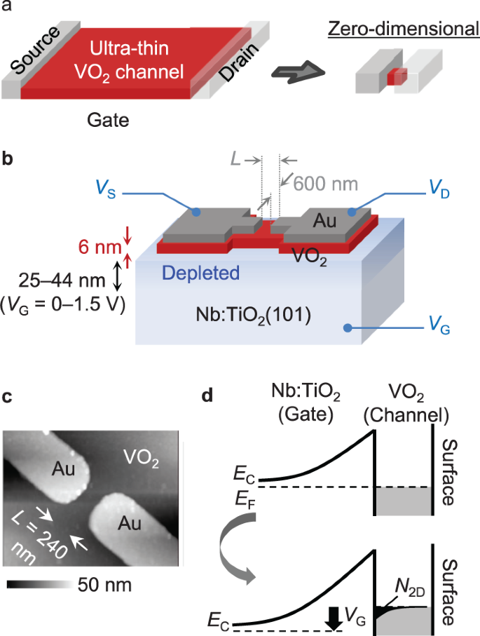
在最先进的工程中,理解纳米尺度的相变是必不可少的1 - 5,而不是简单地平均相变过程中形成的异质畴6,7。然而,随着材料的缩小,相变的陡峭度迅速增加8 - 13,并且在控制方法中要求极高的精度。在这里,一个可以精确控制相变的三端装置(14 - 19)首次应用于缩小的金属-绝缘体过渡材料VO2。澄清了缩小材料从连续跃迁到二元跃迁的交叉,并通过相边界能成功地阐明了临界通道长度。值得注意的是,在临界通道长度以下,空间自由度退化,漏极电压施加的影响在相变中消失,表明VO2通道为零维。这种零维性可能是缩小相变的基本性质,并对需要纳米级工程的各个领域产生重大影响。日本科学家已经证明了控制纳米级器件的原子结构来改变它们的电性能。固体的晶体结构可以随着温度或电场的变化而在原子排列或相之间转换。控制这些相变的器件有可能应用于计算机存储器或传感器,但随着器件变小,这种控制变得越来越困难。来自福冈九州大学的Takeaki Yajima和他的同事们已经在长、薄、亚微米的二氧化钒器件中展示了从金属到绝缘的电诱导变化。该团队表明,当施加电压时,较长的器件在两相之间表现出连续的转变,而亚微米器件出人意料地表现出完全的二进制切换行为。了解这种不同的行为将有助于纳米级电子器件的工程设计。虽然三端器件的静电调谐对于相变材料来说通常是弱的,但它可以比温度或压力更精确地控制相。该技术被应用于按比例缩小的VO2金属-绝缘体过渡,其中材料相由栅极电压控制。利用域边界不稳定性给出了临界通道长度。有趣的是,在临界通道长度以下,非关键刺激(本例中为漏极电压)的影响消失,因为在单畴VO2通道中失去了空间自由度。
本文章由计算机程序翻译,如有差异,请以英文原文为准。

Zero-dimensionality of a scaled-down VO2 metal-insulator transition via high-resolution electrostatic gating

Zero-dimensionality of a scaled-down VO2 metal-insulator transition via high-resolution electrostatic gating

Zero-dimensionality of a scaled-down VO2 metal-insulator transition via high-resolution electrostatic gating
An understanding of the phase transitions at the nanoscale is essential in state-of-the-art engineering1–5, instead of simply averaging the heterogeneous domains formed during phase transitions6,7. However, as materials are scaled down, the steepness of the phase transition rapidly increases8–13 and requires extremely high precision in the control method. Here, a three-terminal device, which could precisely control the phase transition electrically14–19, was applied for the first time to a scaled-down metal-insulator transition material VO2. The crossover from continuous to binary transitions with the scaled-down material was clarified, and the critical channel length was successfully elucidated via phase boundary energy. Notably, below the critical channel length, the spatial degrees of freedom degenerated, and the impact of drain voltage application disappeared in the phase transition, indicating zero-dimensionality of the VO2 channel. This zero-dimensionality could be the fundamental property in the scaled-down phase transition and have a significant impact on various fields that need nanoscale engineering. Controlling the atomic configuration of nanoscale devices to alter their electrical properties has been demonstrated by scientists in Japan. The crystalline structure of a solid can switch between atomic arrangements, or phases, with a change in temperature or electric field. Devices that control these phase transitions have potential applications as computer memories or sensors but such control becomes more difficult as the device gets smaller. Takeaki Yajima from Kyusyu University, Fukuoka, and colleagues have demonstrated the electrically induced change from a metallic to an insulating phase in long, thin, submicrometer vanadium dioxide devices. The team showed that while longer devices exhibited a continuous transition between the two phases as a voltage was applied, the submicrometer devices unexpectedly showed a completely binary switching behavior. Knowing about this different behavior will aid the engineering of nanoscale electronic devices. Although the electrostatic tuning by three-terminal devices is generally weak for phase transition materials, it can control phases with much hither precision than temperature or pressure. This technique was applied to the scaled-down VO2 metal-insulator transitions, where the material phase is controlled by the gate voltage. The crossover from continuous to binary transition with scaling down was demonstrated, and the critical channel length was given by domain boundary instability. Interestingly, below the critical channel length, the influence of the noncritical stimulus (drain voltage in this case) disappeared because the spatial degree of freedom is lost in the single-domain VO2 channel.
求助全文
通过发布文献求助,成功后即可免费获取论文全文。 去求助
来源期刊
Npg Asia Materials
Npg Asia Materials MATERIALS SCIENCE, MULTIDISCIPLINARY-
CiteScore
15.40
自引率
1.00%
发文量
87
审稿时长
2 months
期刊介绍: NPG Asia Materials is an open access, international journal that publishes peer-reviewed review and primary research articles in the field of materials sciences. The journal has a global outlook and reach, with a base in the Asia-Pacific region to reflect the significant and growing output of materials research from this area. The target audience for NPG Asia Materials is scientists and researchers involved in materials research, covering a wide range of disciplines including physical and chemical sciences, biotechnology, and nanotechnology. The journal particularly welcomes high-quality articles from rapidly advancing areas that bridge the gap between materials science and engineering, as well as the classical disciplines of physics, chemistry, and biology. NPG Asia Materials is abstracted/indexed in Journal Citation Reports/Science Edition Web of Knowledge, Google Scholar, Chemical Abstract Services, Scopus, Ulrichsweb (ProQuest), and Scirus.
×
引用
GB/T 7714-2015
复制
MLA
复制
APA
复制
导出至
BibTeX EndNote RefMan NoteFirst NoteExpress
×
提示
您的信息不完整,为了账户安全,请先补充。
现在去补充
×
提示
您因"违规操作"
具体请查看互助需知
我知道了
×
提示
确定
请完成安全验证×
copy
已复制链接
快去分享给好友吧!
我知道了
右上角分享
点击右上角分享
0
联系我们:info@booksci.cn Book学术提供免费学术资源搜索服务,方便国内外学者检索中英文文献。致力于提供最便捷和优质的服务体验。 Copyright © 2023 布克学术 All rights reserved.
京ICP备2023020795号-1
ghs 京公网安备 11010802042870号
Book学术文献互助
Book学术文献互助群
群 号:481959085
Book学术官方微信