Md Naim Jahangir , Jeremy Cleeman , Changqin Pan , Chih-Hung Chang , Rajiv Malhotra
{"title":"Flash辅助3D结构电子学增材制造(FLAME)","authors":"Md Naim Jahangir , Jeremy Cleeman , Changqin Pan , Chih-Hung Chang , Rajiv Malhotra","doi":"10.1016/j.jmapro.2022.08.003","DOIUrl":null,"url":null,"abstract":"<div><p><span><span>Additive integration of 3D electrical circuits with off-the-shelf electronic devices inside 3D printed polymer parts, i.e., structural electronics, can enable new paradigms in miniaturized multifunctional structures. This paper investigates a hybrid printing process called Flash Light Assisted Manufacturing of structural Electronics (FLAME) which integrates Fused Filament Fabrication (FFF) of polymers with printing and Intense Pulsed Light sintering (IPL) of </span>silver nanoparticles. The effect of IPL parameters and nanoparticle shape on conductivity is quantified, revealing that using NWs with IPL allows greater conductivity with lesser sintering-induced polymer damage. The conductivity of planar circuits is characterized during over-FFF, i.e., during FFF of the polymer on the sintered circuit. An unexpected finding is that over-FFF increases the conductivity in a complex and non-monotonic manner that depends on the over-FFF parameters. A multi-layer IPL strategy is introduced for through-plane circuits, in which NWs are deposited in increments smaller than the circuit's total height and IPL is performed after each increment. Electromagnetic and </span>thermal simulations reveal why through-plane circuits have lesser conductivity than planar ones and uncover the key role of multi-layer IPL in increasing the conductivity of through-plane circuits. Overall, FLAME increases the conductivity by 300 % for planar circuits and by 170 % for through-plane circuits as compared to state-of-the-art nanoparticle printing-based methods, even for low-thermal-tolerance polymers, in less than 10 s for each polymer layer. These advances break the performance-material-throughput tradeoff that plagues existing nanoparticle-based printing methods for fabricating 3D structural electronics.</p></div>","PeriodicalId":16148,"journal":{"name":"Journal of Manufacturing Processes","volume":"82 ","pages":"Pages 319-335"},"PeriodicalIF":6.8000,"publicationDate":"2022-10-01","publicationTypes":"Journal Article","fieldsOfStudy":null,"isOpenAccess":false,"openAccessPdf":"","citationCount":"2","resultStr":"{\"title\":\"Flash light assisted additive manufacturing of 3D structural electronics (FLAME)\",\"authors\":\"Md Naim Jahangir , Jeremy Cleeman , Changqin Pan , Chih-Hung Chang , Rajiv Malhotra\",\"doi\":\"10.1016/j.jmapro.2022.08.003\",\"DOIUrl\":null,\"url\":null,\"abstract\":\"<div><p><span><span>Additive integration of 3D electrical circuits with off-the-shelf electronic devices inside 3D printed polymer parts, i.e., structural electronics, can enable new paradigms in miniaturized multifunctional structures. This paper investigates a hybrid printing process called Flash Light Assisted Manufacturing of structural Electronics (FLAME) which integrates Fused Filament Fabrication (FFF) of polymers with printing and Intense Pulsed Light sintering (IPL) of </span>silver nanoparticles. The effect of IPL parameters and nanoparticle shape on conductivity is quantified, revealing that using NWs with IPL allows greater conductivity with lesser sintering-induced polymer damage. The conductivity of planar circuits is characterized during over-FFF, i.e., during FFF of the polymer on the sintered circuit. An unexpected finding is that over-FFF increases the conductivity in a complex and non-monotonic manner that depends on the over-FFF parameters. A multi-layer IPL strategy is introduced for through-plane circuits, in which NWs are deposited in increments smaller than the circuit's total height and IPL is performed after each increment. Electromagnetic and </span>thermal simulations reveal why through-plane circuits have lesser conductivity than planar ones and uncover the key role of multi-layer IPL in increasing the conductivity of through-plane circuits. Overall, FLAME increases the conductivity by 300 % for planar circuits and by 170 % for through-plane circuits as compared to state-of-the-art nanoparticle printing-based methods, even for low-thermal-tolerance polymers, in less than 10 s for each polymer layer. These advances break the performance-material-throughput tradeoff that plagues existing nanoparticle-based printing methods for fabricating 3D structural electronics.</p></div>\",\"PeriodicalId\":16148,\"journal\":{\"name\":\"Journal of Manufacturing Processes\",\"volume\":\"82 \",\"pages\":\"Pages 319-335\"},\"PeriodicalIF\":6.8000,\"publicationDate\":\"2022-10-01\",\"publicationTypes\":\"Journal Article\",\"fieldsOfStudy\":null,\"isOpenAccess\":false,\"openAccessPdf\":\"\",\"citationCount\":\"2\",\"resultStr\":null,\"platform\":\"Semanticscholar\",\"paperid\":null,\"PeriodicalName\":\"Journal of Manufacturing Processes\",\"FirstCategoryId\":\"5\",\"ListUrlMain\":\"https://www.sciencedirect.com/science/article/pii/S1526612522005400\",\"RegionNum\":1,\"RegionCategory\":\"工程技术\",\"ArticlePicture\":[],\"TitleCN\":null,\"AbstractTextCN\":null,\"PMCID\":null,\"EPubDate\":\"\",\"PubModel\":\"\",\"JCR\":\"Q1\",\"JCRName\":\"ENGINEERING, MANUFACTURING\",\"Score\":null,\"Total\":0}","platform":"Semanticscholar","paperid":null,"PeriodicalName":"Journal of Manufacturing Processes","FirstCategoryId":"5","ListUrlMain":"https://www.sciencedirect.com/science/article/pii/S1526612522005400","RegionNum":1,"RegionCategory":"工程技术","ArticlePicture":[],"TitleCN":null,"AbstractTextCN":null,"PMCID":null,"EPubDate":"","PubModel":"","JCR":"Q1","JCRName":"ENGINEERING, MANUFACTURING","Score":null,"Total":0}
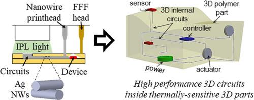
Flash light assisted additive manufacturing of 3D structural electronics (FLAME)
Additive integration of 3D electrical circuits with off-the-shelf electronic devices inside 3D printed polymer parts, i.e., structural electronics, can enable new paradigms in miniaturized multifunctional structures. This paper investigates a hybrid printing process called Flash Light Assisted Manufacturing of structural Electronics (FLAME) which integrates Fused Filament Fabrication (FFF) of polymers with printing and Intense Pulsed Light sintering (IPL) of silver nanoparticles. The effect of IPL parameters and nanoparticle shape on conductivity is quantified, revealing that using NWs with IPL allows greater conductivity with lesser sintering-induced polymer damage. The conductivity of planar circuits is characterized during over-FFF, i.e., during FFF of the polymer on the sintered circuit. An unexpected finding is that over-FFF increases the conductivity in a complex and non-monotonic manner that depends on the over-FFF parameters. A multi-layer IPL strategy is introduced for through-plane circuits, in which NWs are deposited in increments smaller than the circuit's total height and IPL is performed after each increment. Electromagnetic and thermal simulations reveal why through-plane circuits have lesser conductivity than planar ones and uncover the key role of multi-layer IPL in increasing the conductivity of through-plane circuits. Overall, FLAME increases the conductivity by 300 % for planar circuits and by 170 % for through-plane circuits as compared to state-of-the-art nanoparticle printing-based methods, even for low-thermal-tolerance polymers, in less than 10 s for each polymer layer. These advances break the performance-material-throughput tradeoff that plagues existing nanoparticle-based printing methods for fabricating 3D structural electronics.
期刊介绍:
The aim of the Journal of Manufacturing Processes (JMP) is to exchange current and future directions of manufacturing processes research, development and implementation, and to publish archival scholarly literature with a view to advancing state-of-the-art manufacturing processes and encouraging innovation for developing new and efficient processes. The journal will also publish from other research communities for rapid communication of innovative new concepts. Special-topic issues on emerging technologies and invited papers will also be published.

 求助内容:
求助内容: 应助结果提醒方式:


