Qun Cao, Zijun Shao, Dale Hensley and B. Jill Venton
{"title":"用于测量神经递质的碳纳米刺涂层纳米电极†","authors":"Qun Cao, Zijun Shao, Dale Hensley and B. Jill Venton","doi":"10.1039/D1FD00053E","DOIUrl":null,"url":null,"abstract":"<p >Carbon nanoelectrodes enable the detection of neurotransmitters at the level of single cells, vesicles, synapses and small brain structures. Previously, the etching of carbon fibers and 3D printing based on direct laser writing have been used to fabricate carbon nanoelectrodes, but these methods lack the ability of mass manufacturing. In this paper, we mass fabricate carbon nanoelectrodes by growing carbon nanospikes (CNSs) on metal wires. CNSs have a short, dense and defect-rich surface that produces remarkable electrochemical properties, and they can be mass fabricated on almost any substrate without using catalysts. Tungsten wires and niobium wires were electrochemically etched in batch to form sub micrometer sized tips, and a layer of CNSs was grown on the metal wires using plasma-enhanced chemical vapor deposition (PE-CVD). The thickness of the CNS layer was controlled by the deposition time, and a thin layer of CNSs can effectively cover the entire metal surface while maintaining the tip size within the sub micrometer scale. The etched tungsten wires produced tapered conical nanotips, while the etched niobium wires were long and thin. Both showed excellent sensitivity for the detection of outer sphere ruthenium hexamine and the inner sphere test compound ferricyanide. The CNS nanosensors were used for the measurement of dopamine, serotonin, ascorbic acid and DOPAC with fast-scan cyclic voltammetry. The CNS nanoelectrodes had a large surface area and numerous defect sites, which improved the sensitivity, electron transfer kinetics and adsorption. Finally, the CNS nanoelectrodes were compared with other nanoelectrode fabrication methods, including flame etching, 3D printing, and nanopipettes, which are slower to make and more difficult for mass fabrication. Thus, CNS nanoelectrodes are a promising strategy for the mass fabrication of nanoelectrode sensors for neurotransmitters.</p>","PeriodicalId":76,"journal":{"name":"Faraday Discussions","volume":"233 ","pages":" 303-314"},"PeriodicalIF":3.1000,"publicationDate":"2021-12-10","publicationTypes":"Journal Article","fieldsOfStudy":null,"isOpenAccess":false,"openAccessPdf":"https://pubs.rsc.org/en/content/articlepdf/2022/fd/d1fd00053e?page=search","citationCount":"4","resultStr":"{\"title\":\"Carbon nanospike coated nanoelectrodes for measurements of neurotransmitters†\",\"authors\":\"Qun Cao, Zijun Shao, Dale Hensley and B. Jill Venton\",\"doi\":\"10.1039/D1FD00053E\",\"DOIUrl\":null,\"url\":null,\"abstract\":\"<p >Carbon nanoelectrodes enable the detection of neurotransmitters at the level of single cells, vesicles, synapses and small brain structures. Previously, the etching of carbon fibers and 3D printing based on direct laser writing have been used to fabricate carbon nanoelectrodes, but these methods lack the ability of mass manufacturing. In this paper, we mass fabricate carbon nanoelectrodes by growing carbon nanospikes (CNSs) on metal wires. CNSs have a short, dense and defect-rich surface that produces remarkable electrochemical properties, and they can be mass fabricated on almost any substrate without using catalysts. Tungsten wires and niobium wires were electrochemically etched in batch to form sub micrometer sized tips, and a layer of CNSs was grown on the metal wires using plasma-enhanced chemical vapor deposition (PE-CVD). The thickness of the CNS layer was controlled by the deposition time, and a thin layer of CNSs can effectively cover the entire metal surface while maintaining the tip size within the sub micrometer scale. The etched tungsten wires produced tapered conical nanotips, while the etched niobium wires were long and thin. Both showed excellent sensitivity for the detection of outer sphere ruthenium hexamine and the inner sphere test compound ferricyanide. The CNS nanosensors were used for the measurement of dopamine, serotonin, ascorbic acid and DOPAC with fast-scan cyclic voltammetry. The CNS nanoelectrodes had a large surface area and numerous defect sites, which improved the sensitivity, electron transfer kinetics and adsorption. Finally, the CNS nanoelectrodes were compared with other nanoelectrode fabrication methods, including flame etching, 3D printing, and nanopipettes, which are slower to make and more difficult for mass fabrication. Thus, CNS nanoelectrodes are a promising strategy for the mass fabrication of nanoelectrode sensors for neurotransmitters.</p>\",\"PeriodicalId\":76,\"journal\":{\"name\":\"Faraday Discussions\",\"volume\":\"233 \",\"pages\":\" 303-314\"},\"PeriodicalIF\":3.1000,\"publicationDate\":\"2021-12-10\",\"publicationTypes\":\"Journal Article\",\"fieldsOfStudy\":null,\"isOpenAccess\":false,\"openAccessPdf\":\"https://pubs.rsc.org/en/content/articlepdf/2022/fd/d1fd00053e?page=search\",\"citationCount\":\"4\",\"resultStr\":null,\"platform\":\"Semanticscholar\",\"paperid\":null,\"PeriodicalName\":\"Faraday Discussions\",\"FirstCategoryId\":\"92\",\"ListUrlMain\":\"https://pubs.rsc.org/en/content/articlelanding/2022/fd/d1fd00053e\",\"RegionNum\":3,\"RegionCategory\":\"化学\",\"ArticlePicture\":[],\"TitleCN\":null,\"AbstractTextCN\":null,\"PMCID\":null,\"EPubDate\":\"\",\"PubModel\":\"\",\"JCR\":\"Q2\",\"JCRName\":\"CHEMISTRY, PHYSICAL\",\"Score\":null,\"Total\":0}","platform":"Semanticscholar","paperid":null,"PeriodicalName":"Faraday Discussions","FirstCategoryId":"92","ListUrlMain":"https://pubs.rsc.org/en/content/articlelanding/2022/fd/d1fd00053e","RegionNum":3,"RegionCategory":"化学","ArticlePicture":[],"TitleCN":null,"AbstractTextCN":null,"PMCID":null,"EPubDate":"","PubModel":"","JCR":"Q2","JCRName":"CHEMISTRY, PHYSICAL","Score":null,"Total":0}
Carbon nanospike coated nanoelectrodes for measurements of neurotransmitters†
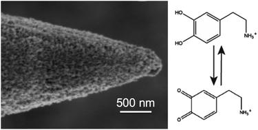
Carbon nanoelectrodes enable the detection of neurotransmitters at the level of single cells, vesicles, synapses and small brain structures. Previously, the etching of carbon fibers and 3D printing based on direct laser writing have been used to fabricate carbon nanoelectrodes, but these methods lack the ability of mass manufacturing. In this paper, we mass fabricate carbon nanoelectrodes by growing carbon nanospikes (CNSs) on metal wires. CNSs have a short, dense and defect-rich surface that produces remarkable electrochemical properties, and they can be mass fabricated on almost any substrate without using catalysts. Tungsten wires and niobium wires were electrochemically etched in batch to form sub micrometer sized tips, and a layer of CNSs was grown on the metal wires using plasma-enhanced chemical vapor deposition (PE-CVD). The thickness of the CNS layer was controlled by the deposition time, and a thin layer of CNSs can effectively cover the entire metal surface while maintaining the tip size within the sub micrometer scale. The etched tungsten wires produced tapered conical nanotips, while the etched niobium wires were long and thin. Both showed excellent sensitivity for the detection of outer sphere ruthenium hexamine and the inner sphere test compound ferricyanide. The CNS nanosensors were used for the measurement of dopamine, serotonin, ascorbic acid and DOPAC with fast-scan cyclic voltammetry. The CNS nanoelectrodes had a large surface area and numerous defect sites, which improved the sensitivity, electron transfer kinetics and adsorption. Finally, the CNS nanoelectrodes were compared with other nanoelectrode fabrication methods, including flame etching, 3D printing, and nanopipettes, which are slower to make and more difficult for mass fabrication. Thus, CNS nanoelectrodes are a promising strategy for the mass fabrication of nanoelectrode sensors for neurotransmitters.

 求助内容:
求助内容: 应助结果提醒方式:


