S. G. Petrosyan, A. S. Musayelyan, A. S. Tokmajyan, V. F. Gremenok, A. V. Stanchik, K. P. Buskis, O.V. Korolik
{"title":"化学浴沉积法在聚酰亚胺衬底上制备CdS薄膜","authors":"S. G. Petrosyan, A. S. Musayelyan, A. S. Tokmajyan, V. F. Gremenok, A. V. Stanchik, K. P. Buskis, O.V. Korolik","doi":"10.1134/S1068337225700549","DOIUrl":null,"url":null,"abstract":"<p>Thin films of polycrystalline cadmium sulfide (CdS) were deposited on polyimide substrates using the chemical bath deposition method at a fixed solution temperature of (62 ± 1)°C. The influence of deposition time on the structural and optical properties of the resulting thin films was studied in detail. X-ray diffraction (XRD) revealed that the films predominantly consist of the hexagonal phase of CdS, with a crystallite size of approximately 10 nm, which slightly decreases with increasing deposition time. The surface roughness of the films was measured using atomic force microscopy. Scanning electron microscopy showed a uniform, compact, and smooth film surface. Raman measurements revealed three main peaks corresponding to the 1LO, 2LO, and 3LO modes in CdS. Optical measurements showed a high transmittance coefficient (~85%) and a low reflectance coefficient (4–7%) in the spectral range of 520–1000 nm. Due to changes in the stoichiometry of the CdS films, the optical band gap varied within the range of 2.30–2.37 eV with increasing deposition time. Room temperature photoluminescence spectra of the films exhibited two emission peaks located at 500 nm (2.49 eV) and 708 nm (1.75 eV), which can be attributed to free carrier recombination and excitonic or radiative transitions involving donor and acceptor levels, respectively. The obtained results demonstrate that by controlling only the deposition time, it is possible to deposit CdS thin films on polymer substrates at a relatively low chemical bath temperature. These films, without any post-growth treatment, possess sufficiently good physical properties, making them suitable for use in various flexible optoelectronic devices.</p>","PeriodicalId":623,"journal":{"name":"Journal of Contemporary Physics (Armenian Academy of Sciences)","volume":"60 2","pages":"210 - 221"},"PeriodicalIF":0.4000,"publicationDate":"2025-10-07","publicationTypes":"Journal Article","fieldsOfStudy":null,"isOpenAccess":false,"openAccessPdf":"","citationCount":"0","resultStr":"{\"title\":\"Thin Films of CdS Formed on a Polyimide Substrate by Chemical Bath Deposition Method\",\"authors\":\"S. G. Petrosyan, A. S. Musayelyan, A. S. Tokmajyan, V. F. Gremenok, A. V. Stanchik, K. P. Buskis, O.V. Korolik\",\"doi\":\"10.1134/S1068337225700549\",\"DOIUrl\":null,\"url\":null,\"abstract\":\"<p>Thin films of polycrystalline cadmium sulfide (CdS) were deposited on polyimide substrates using the chemical bath deposition method at a fixed solution temperature of (62 ± 1)°C. The influence of deposition time on the structural and optical properties of the resulting thin films was studied in detail. X-ray diffraction (XRD) revealed that the films predominantly consist of the hexagonal phase of CdS, with a crystallite size of approximately 10 nm, which slightly decreases with increasing deposition time. The surface roughness of the films was measured using atomic force microscopy. Scanning electron microscopy showed a uniform, compact, and smooth film surface. Raman measurements revealed three main peaks corresponding to the 1LO, 2LO, and 3LO modes in CdS. Optical measurements showed a high transmittance coefficient (~85%) and a low reflectance coefficient (4–7%) in the spectral range of 520–1000 nm. Due to changes in the stoichiometry of the CdS films, the optical band gap varied within the range of 2.30–2.37 eV with increasing deposition time. Room temperature photoluminescence spectra of the films exhibited two emission peaks located at 500 nm (2.49 eV) and 708 nm (1.75 eV), which can be attributed to free carrier recombination and excitonic or radiative transitions involving donor and acceptor levels, respectively. The obtained results demonstrate that by controlling only the deposition time, it is possible to deposit CdS thin films on polymer substrates at a relatively low chemical bath temperature. These films, without any post-growth treatment, possess sufficiently good physical properties, making them suitable for use in various flexible optoelectronic devices.</p>\",\"PeriodicalId\":623,\"journal\":{\"name\":\"Journal of Contemporary Physics (Armenian Academy of Sciences)\",\"volume\":\"60 2\",\"pages\":\"210 - 221\"},\"PeriodicalIF\":0.4000,\"publicationDate\":\"2025-10-07\",\"publicationTypes\":\"Journal Article\",\"fieldsOfStudy\":null,\"isOpenAccess\":false,\"openAccessPdf\":\"\",\"citationCount\":\"0\",\"resultStr\":null,\"platform\":\"Semanticscholar\",\"paperid\":null,\"PeriodicalName\":\"Journal of Contemporary Physics (Armenian Academy of Sciences)\",\"FirstCategoryId\":\"101\",\"ListUrlMain\":\"https://link.springer.com/article/10.1134/S1068337225700549\",\"RegionNum\":4,\"RegionCategory\":\"物理与天体物理\",\"ArticlePicture\":[],\"TitleCN\":null,\"AbstractTextCN\":null,\"PMCID\":null,\"EPubDate\":\"\",\"PubModel\":\"\",\"JCR\":\"Q4\",\"JCRName\":\"PHYSICS, MULTIDISCIPLINARY\",\"Score\":null,\"Total\":0}","platform":"Semanticscholar","paperid":null,"PeriodicalName":"Journal of Contemporary Physics (Armenian Academy of Sciences)","FirstCategoryId":"101","ListUrlMain":"https://link.springer.com/article/10.1134/S1068337225700549","RegionNum":4,"RegionCategory":"物理与天体物理","ArticlePicture":[],"TitleCN":null,"AbstractTextCN":null,"PMCID":null,"EPubDate":"","PubModel":"","JCR":"Q4","JCRName":"PHYSICS, MULTIDISCIPLINARY","Score":null,"Total":0}
Thin Films of CdS Formed on a Polyimide Substrate by Chemical Bath Deposition Method
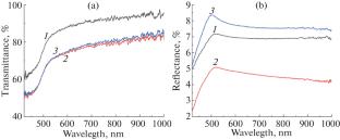
Thin films of polycrystalline cadmium sulfide (CdS) were deposited on polyimide substrates using the chemical bath deposition method at a fixed solution temperature of (62 ± 1)°C. The influence of deposition time on the structural and optical properties of the resulting thin films was studied in detail. X-ray diffraction (XRD) revealed that the films predominantly consist of the hexagonal phase of CdS, with a crystallite size of approximately 10 nm, which slightly decreases with increasing deposition time. The surface roughness of the films was measured using atomic force microscopy. Scanning electron microscopy showed a uniform, compact, and smooth film surface. Raman measurements revealed three main peaks corresponding to the 1LO, 2LO, and 3LO modes in CdS. Optical measurements showed a high transmittance coefficient (~85%) and a low reflectance coefficient (4–7%) in the spectral range of 520–1000 nm. Due to changes in the stoichiometry of the CdS films, the optical band gap varied within the range of 2.30–2.37 eV with increasing deposition time. Room temperature photoluminescence spectra of the films exhibited two emission peaks located at 500 nm (2.49 eV) and 708 nm (1.75 eV), which can be attributed to free carrier recombination and excitonic or radiative transitions involving donor and acceptor levels, respectively. The obtained results demonstrate that by controlling only the deposition time, it is possible to deposit CdS thin films on polymer substrates at a relatively low chemical bath temperature. These films, without any post-growth treatment, possess sufficiently good physical properties, making them suitable for use in various flexible optoelectronic devices.
期刊介绍:
Journal of Contemporary Physics (Armenian Academy of Sciences) is a journal that covers all fields of modern physics. It publishes significant contributions in such areas of theoretical and applied science as interaction of elementary particles at superhigh energies, elementary particle physics, charged particle interactions with matter, physics of semiconductors and semiconductor devices, physics of condensed matter, radiophysics and radioelectronics, optics and quantum electronics, quantum size effects, nanophysics, sensorics, and superconductivity.
 求助内容:
求助内容: 应助结果提醒方式:


