Jianjie Li, Yu Xu, Jianxi Xu, Miao Liu, Tian Xia, Jiangpeng Zhu, Yizhe Huang, Liang Wang, Lei Yao, Jianfeng Wang, Bing Cao and Ke Xu
{"title":"半导体化合物二维材料辅助外延的研究进展及应用","authors":"Jianjie Li, Yu Xu, Jianxi Xu, Miao Liu, Tian Xia, Jiangpeng Zhu, Yizhe Huang, Liang Wang, Lei Yao, Jianfeng Wang, Bing Cao and Ke Xu","doi":"10.1039/D5CE00546A","DOIUrl":null,"url":null,"abstract":"<p >The groundbreaking development of semiconductor thin-film materials has played a pivotal role in advancing modern technologies, with extensive applications spanning lighting displays, power electronics, and microwave/RF systems. In vapor-phase epitaxy, the innovative integration of two-dimensional (2D) materials offers revolutionary solutions to address lattice mismatch and thermal expansion mismatch in heteroepitaxial growth: weak van der Waals interactions at interfaces effectively mitigate stress accumulation, while surface state engineering of 2D materials enables precise control over nucleation dynamics. Furthermore, the synergistic relationship between the layer number of 2D materials and substrate polarity allows directional modulation of epitaxial growth. Notably, the breakthrough in detachable transfer of epitaxial layers has unlocked new possibilities for flexible electronics and hybrid integrated devices. This study systematically investigates the unique advantages of 2D materials in optimizing epitaxial growth and expanding device functionalities. By analyzing the heteroepitaxial characteristics of ZnO, GaAs, GaN, and AlN on 2D materials, along with their optoelectronic and high-frequency device applications, we provide a theoretical framework and practical guidance to overcome current technological limitations and outline future research directions.</p>","PeriodicalId":70,"journal":{"name":"CrystEngComm","volume":" 37","pages":" 6088-6105"},"PeriodicalIF":2.6000,"publicationDate":"2025-09-04","publicationTypes":"Journal Article","fieldsOfStudy":null,"isOpenAccess":false,"openAccessPdf":"","citationCount":"0","resultStr":"{\"title\":\"Advancements and applications in two-dimensional material-assisted epitaxy of semiconductor compounds\",\"authors\":\"Jianjie Li, Yu Xu, Jianxi Xu, Miao Liu, Tian Xia, Jiangpeng Zhu, Yizhe Huang, Liang Wang, Lei Yao, Jianfeng Wang, Bing Cao and Ke Xu\",\"doi\":\"10.1039/D5CE00546A\",\"DOIUrl\":null,\"url\":null,\"abstract\":\"<p >The groundbreaking development of semiconductor thin-film materials has played a pivotal role in advancing modern technologies, with extensive applications spanning lighting displays, power electronics, and microwave/RF systems. In vapor-phase epitaxy, the innovative integration of two-dimensional (2D) materials offers revolutionary solutions to address lattice mismatch and thermal expansion mismatch in heteroepitaxial growth: weak van der Waals interactions at interfaces effectively mitigate stress accumulation, while surface state engineering of 2D materials enables precise control over nucleation dynamics. Furthermore, the synergistic relationship between the layer number of 2D materials and substrate polarity allows directional modulation of epitaxial growth. Notably, the breakthrough in detachable transfer of epitaxial layers has unlocked new possibilities for flexible electronics and hybrid integrated devices. This study systematically investigates the unique advantages of 2D materials in optimizing epitaxial growth and expanding device functionalities. By analyzing the heteroepitaxial characteristics of ZnO, GaAs, GaN, and AlN on 2D materials, along with their optoelectronic and high-frequency device applications, we provide a theoretical framework and practical guidance to overcome current technological limitations and outline future research directions.</p>\",\"PeriodicalId\":70,\"journal\":{\"name\":\"CrystEngComm\",\"volume\":\" 37\",\"pages\":\" 6088-6105\"},\"PeriodicalIF\":2.6000,\"publicationDate\":\"2025-09-04\",\"publicationTypes\":\"Journal Article\",\"fieldsOfStudy\":null,\"isOpenAccess\":false,\"openAccessPdf\":\"\",\"citationCount\":\"0\",\"resultStr\":null,\"platform\":\"Semanticscholar\",\"paperid\":null,\"PeriodicalName\":\"CrystEngComm\",\"FirstCategoryId\":\"92\",\"ListUrlMain\":\"https://pubs.rsc.org/en/content/articlelanding/2025/ce/d5ce00546a\",\"RegionNum\":3,\"RegionCategory\":\"化学\",\"ArticlePicture\":[],\"TitleCN\":null,\"AbstractTextCN\":null,\"PMCID\":null,\"EPubDate\":\"\",\"PubModel\":\"\",\"JCR\":\"Q2\",\"JCRName\":\"CHEMISTRY, MULTIDISCIPLINARY\",\"Score\":null,\"Total\":0}","platform":"Semanticscholar","paperid":null,"PeriodicalName":"CrystEngComm","FirstCategoryId":"92","ListUrlMain":"https://pubs.rsc.org/en/content/articlelanding/2025/ce/d5ce00546a","RegionNum":3,"RegionCategory":"化学","ArticlePicture":[],"TitleCN":null,"AbstractTextCN":null,"PMCID":null,"EPubDate":"","PubModel":"","JCR":"Q2","JCRName":"CHEMISTRY, MULTIDISCIPLINARY","Score":null,"Total":0}
Advancements and applications in two-dimensional material-assisted epitaxy of semiconductor compounds
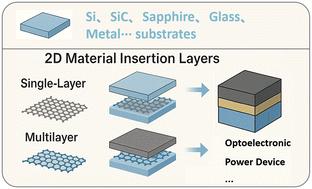
The groundbreaking development of semiconductor thin-film materials has played a pivotal role in advancing modern technologies, with extensive applications spanning lighting displays, power electronics, and microwave/RF systems. In vapor-phase epitaxy, the innovative integration of two-dimensional (2D) materials offers revolutionary solutions to address lattice mismatch and thermal expansion mismatch in heteroepitaxial growth: weak van der Waals interactions at interfaces effectively mitigate stress accumulation, while surface state engineering of 2D materials enables precise control over nucleation dynamics. Furthermore, the synergistic relationship between the layer number of 2D materials and substrate polarity allows directional modulation of epitaxial growth. Notably, the breakthrough in detachable transfer of epitaxial layers has unlocked new possibilities for flexible electronics and hybrid integrated devices. This study systematically investigates the unique advantages of 2D materials in optimizing epitaxial growth and expanding device functionalities. By analyzing the heteroepitaxial characteristics of ZnO, GaAs, GaN, and AlN on 2D materials, along with their optoelectronic and high-frequency device applications, we provide a theoretical framework and practical guidance to overcome current technological limitations and outline future research directions.
 求助内容:
求助内容: 应助结果提醒方式:


