深入分析由晶体半导体制成的硼纳米纤维的结构、光学、电学和磁性能
IF 4.7
3区 材料科学
Q2 MATERIALS SCIENCE, MULTIDISCIPLINARY
引用次数: 0
摘要
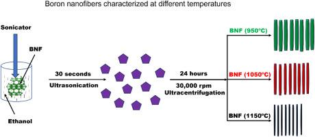
本文报道了用双脉冲激光烧蚀(DPLA)方法在950、1050和1150℃的温度下合成晶体半导体硼纳米纤维(BNF)的结构、光学、电学和磁性能。本研究旨在利用不同的分析技术来表征和研究BNF的性质。高分辨率透射电子显微镜(HRTEM)和场发射扫描电子显微镜(FESEM)显示,BNF的宽度为5 ~ 100 nm,长度为1 ~ 5 μm。各BNF的紫外-可见吸收光谱分别在290、300和310 nm处有明显的吸收峰。BNF的光致发光(PL)测量显示,在447、448和450 nm处有一个强峰,与它们的发射峰相对应。Tauc图计算表明,与带隙为1.90 eV的块状硼相比,每个BNF都表现出直接跃迁,证实了它们随带隙增加而具有半导体性质。振动样品磁强计(VSM)测量显示了BNF的矫顽力磁性值,使其可用于存储器件。对BNF的电导率进行了测量,结果表明BNF的电导率比硼粉高,这是由于其平面内电子传递增强所致。傅里叶红外光谱(FTIR)分析表明,复合材料的每个BNF上都存在氢化物、氧化物、氢氧化物和氧官能团。根据不同参数获得的结果,制备的BNF适用于各种应用,如电子,储氢,组织工程,药物输送系统,辐射屏蔽和中子捕获治疗。本文章由计算机程序翻译,如有差异,请以英文原文为准。
In-depth analysis of the structural, optical, electrical, and magnetic properties of boron nanofibers made from crystalline semiconductors
The study reports on the structural, optical, electrical, and magnetic properties of crystalline semiconductor boron nanofibers (BNF) synthesized at temperatures of 950, 1050, and 1150 °C using the dual pulsed laser ablation (DPLA) method from bulk boron. This study aims to characterize and investigate the properties of the BNF using different analytical techniques. High-resolution transmission electron microscopy (HRTEM) and field emission scanning electron microscopy (FESEM) revealed that the BNF had a width ranging from 5 to 100 nm and a length between 1 and 5 μm. Each BNF's ultraviolet–visible (UV–Vis) absorption spectra exhibited a distinct absorption peak at 290, 300, and 310 nm, respectively. Photoluminescence (PL) measurements of the BNF showed a strong peak at 447, 448, and 450 nm, corresponding to their emission peak. Tauc plot calculations indicated that each BNF displayed a direct transition, confirming their semiconductor nature with the increase in band gaps, compared to bulk boron with a band gap of 1.90 eV. The vibrating sample magnetometer (VSM) measurements revealed coercivity magnetic values of the BNF, making them useful for storage devices. The electrical conductivity of the BNF was measured, showing higher conductivity than boron powder due to enhanced in-plane electron transport. Fourier-transform infrared spectroscopy (FTIR) analysis indicated the presence of hydrides, oxides, hydroxides, and oxy-functional groups on each BNF for composite materials. Based on the results obtained from different parameters, the BNF prepared are suitable for various applications, such as electronics, hydrogen storage, tissue engineering, drug delivery systems, radiation shielding, and neutron capture therapy.
求助全文
通过发布文献求助,成功后即可免费获取论文全文。
去求助
来源期刊
Materials Chemistry and Physics
工程技术-材料科学:综合
CiteScore
8.70
自引率
4.30%
发文量
1515
审稿时长
69 days
期刊介绍:
Materials Chemistry and Physics is devoted to short communications, full-length research papers and feature articles on interrelationships among structure, properties, processing and performance of materials. The Editors welcome manuscripts on thin films, surface and interface science, materials degradation and reliability, metallurgy, semiconductors and optoelectronic materials, fine ceramics, magnetics, superconductors, specialty polymers, nano-materials and composite materials.
 求助内容:
求助内容: 应助结果提醒方式:


