宽禁带半导体晶圆的物理化学辅助纳米制造技术综述

IF 18.8 1区 工程技术 Q1 ENGINEERING, MANUFACTURING
Kazuya Yamamura , Hui Deng , Yasuhisa Sano , Junji Murata , Xu Yang , Rongyan Sun
{"title":"宽禁带半导体晶圆的物理化学辅助纳米制造技术综述","authors":"Kazuya Yamamura ,&nbsp;Hui Deng ,&nbsp;Yasuhisa Sano ,&nbsp;Junji Murata ,&nbsp;Xu Yang ,&nbsp;Rongyan Sun","doi":"10.1016/j.ijmachtools.2025.104321","DOIUrl":null,"url":null,"abstract":"<div><div>Nanomanufacturing involves not only fabricating nanoscale three-dimensional microstructures but also achieving nanoscale surface planarization and smoothing—an indispensable requirement in semiconductor-wafer processing. Wide-bandgap semiconductors such as SiC, GaN, diamond, and AlN combine high hardness, brittleness, and chemical inertness, making it exceptionally difficult to produce large size wafers with damage-free, atomic-level smoothness that meets the performance demands of next-generation devices. Physical–chemical composite methods, which marry the high-efficiency planarization of mechanical removal with the damage-free of chemical reactions, have emerged as the most promising route to overcome this challenge. Chemical mechanical polishing (CMP), the first-generation composite technique, was well established in industry; however, its low material removal rates, extensive consumable use, and environmental burden were increasingly problematic as wafer sizes grow and new wide-bandgap materials become mainstream. This review surveys the principal physicochemical processing techniques and examines four representative approaches—plasma-assisted polishing (PAP), plasma-based atomic-selective etching (PASE), catalyst-assisted etching (CARE), and electrochemical mechanical polishing (ECMP). A systematic comparison of their mechanisms, advantages, and limitations clarifies how these methods maintain crystal integrity while enabling selective material removal, thereby delivering atomically smooth surfaces with significantly higher throughput. The review provides both theoretical insight and practical guidance for cost-effective, atomically precise processing of wide-bandgap semiconductor wafers.</div></div>","PeriodicalId":14011,"journal":{"name":"International Journal of Machine Tools & Manufacture","volume":"211 ","pages":"Article 104321"},"PeriodicalIF":18.8000,"publicationDate":"2025-08-12","publicationTypes":"Journal Article","fieldsOfStudy":null,"isOpenAccess":false,"openAccessPdf":"","citationCount":"0","resultStr":"{\"title\":\"Review of physicochemical-assisted nanomanufacturing processes for wide-bandgap semiconductor wafers\",\"authors\":\"Kazuya Yamamura ,&nbsp;Hui Deng ,&nbsp;Yasuhisa Sano ,&nbsp;Junji Murata ,&nbsp;Xu Yang ,&nbsp;Rongyan Sun\",\"doi\":\"10.1016/j.ijmachtools.2025.104321\",\"DOIUrl\":null,\"url\":null,\"abstract\":\"<div><div>Nanomanufacturing involves not only fabricating nanoscale three-dimensional microstructures but also achieving nanoscale surface planarization and smoothing—an indispensable requirement in semiconductor-wafer processing. Wide-bandgap semiconductors such as SiC, GaN, diamond, and AlN combine high hardness, brittleness, and chemical inertness, making it exceptionally difficult to produce large size wafers with damage-free, atomic-level smoothness that meets the performance demands of next-generation devices. Physical–chemical composite methods, which marry the high-efficiency planarization of mechanical removal with the damage-free of chemical reactions, have emerged as the most promising route to overcome this challenge. Chemical mechanical polishing (CMP), the first-generation composite technique, was well established in industry; however, its low material removal rates, extensive consumable use, and environmental burden were increasingly problematic as wafer sizes grow and new wide-bandgap materials become mainstream. This review surveys the principal physicochemical processing techniques and examines four representative approaches—plasma-assisted polishing (PAP), plasma-based atomic-selective etching (PASE), catalyst-assisted etching (CARE), and electrochemical mechanical polishing (ECMP). A systematic comparison of their mechanisms, advantages, and limitations clarifies how these methods maintain crystal integrity while enabling selective material removal, thereby delivering atomically smooth surfaces with significantly higher throughput. The review provides both theoretical insight and practical guidance for cost-effective, atomically precise processing of wide-bandgap semiconductor wafers.</div></div>\",\"PeriodicalId\":14011,\"journal\":{\"name\":\"International Journal of Machine Tools & Manufacture\",\"volume\":\"211 \",\"pages\":\"Article 104321\"},\"PeriodicalIF\":18.8000,\"publicationDate\":\"2025-08-12\",\"publicationTypes\":\"Journal Article\",\"fieldsOfStudy\":null,\"isOpenAccess\":false,\"openAccessPdf\":\"\",\"citationCount\":\"0\",\"resultStr\":null,\"platform\":\"Semanticscholar\",\"paperid\":null,\"PeriodicalName\":\"International Journal of Machine Tools & Manufacture\",\"FirstCategoryId\":\"5\",\"ListUrlMain\":\"https://www.sciencedirect.com/science/article/pii/S0890695525000768\",\"RegionNum\":1,\"RegionCategory\":\"工程技术\",\"ArticlePicture\":[],\"TitleCN\":null,\"AbstractTextCN\":null,\"PMCID\":null,\"EPubDate\":\"\",\"PubModel\":\"\",\"JCR\":\"Q1\",\"JCRName\":\"ENGINEERING, MANUFACTURING\",\"Score\":null,\"Total\":0}","platform":"Semanticscholar","paperid":null,"PeriodicalName":"International Journal of Machine Tools & Manufacture","FirstCategoryId":"5","ListUrlMain":"https://www.sciencedirect.com/science/article/pii/S0890695525000768","RegionNum":1,"RegionCategory":"工程技术","ArticlePicture":[],"TitleCN":null,"AbstractTextCN":null,"PMCID":null,"EPubDate":"","PubModel":"","JCR":"Q1","JCRName":"ENGINEERING, MANUFACTURING","Score":null,"Total":0}
引用次数: 0

摘要

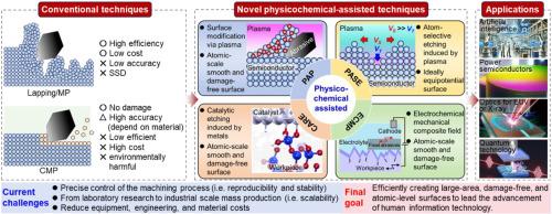
纳米制造不仅涉及制造纳米级三维微结构,还涉及实现纳米级表面平面化和光滑化,这是半导体晶圆加工中不可或缺的要求。宽带隙半导体,如SiC、GaN、金刚石和AlN,结合了高硬度、脆性和化学惰性,使得生产具有无损伤、原子级光滑度的大尺寸晶圆,满足下一代器件的性能要求,变得异常困难。物理化学复合方法结合了机械去除的高效率平面化和化学反应的无损伤性,已经成为克服这一挑战的最有希望的途径。化学机械抛光(CMP)是第一代复合材料技术,在工业上已经得到了很好的应用;然而,随着晶圆尺寸的增长和新型宽带隙材料的主流化,其材料去除率低、耗材广泛以及环境负担日益成为问题。本文综述了主要的物理化学加工技术,并研究了四种具有代表性的方法——等离子体辅助抛光(PAP)、等离子体基原子选择性蚀刻(PASE)、催化剂辅助蚀刻(CARE)和电化学机械抛光(ECMP)。系统地比较了它们的机制、优点和局限性,阐明了这些方法如何在实现选择性材料去除的同时保持晶体完整性,从而提供具有显着更高吞吐量的原子光滑表面。该综述为低成本、原子精度高的宽禁带半导体晶圆加工提供了理论见解和实践指导。
本文章由计算机程序翻译,如有差异,请以英文原文为准。

Review of physicochemical-assisted nanomanufacturing processes for wide-bandgap semiconductor wafers

Review of physicochemical-assisted nanomanufacturing processes for wide-bandgap semiconductor wafers
Nanomanufacturing involves not only fabricating nanoscale three-dimensional microstructures but also achieving nanoscale surface planarization and smoothing—an indispensable requirement in semiconductor-wafer processing. Wide-bandgap semiconductors such as SiC, GaN, diamond, and AlN combine high hardness, brittleness, and chemical inertness, making it exceptionally difficult to produce large size wafers with damage-free, atomic-level smoothness that meets the performance demands of next-generation devices. Physical–chemical composite methods, which marry the high-efficiency planarization of mechanical removal with the damage-free of chemical reactions, have emerged as the most promising route to overcome this challenge. Chemical mechanical polishing (CMP), the first-generation composite technique, was well established in industry; however, its low material removal rates, extensive consumable use, and environmental burden were increasingly problematic as wafer sizes grow and new wide-bandgap materials become mainstream. This review surveys the principal physicochemical processing techniques and examines four representative approaches—plasma-assisted polishing (PAP), plasma-based atomic-selective etching (PASE), catalyst-assisted etching (CARE), and electrochemical mechanical polishing (ECMP). A systematic comparison of their mechanisms, advantages, and limitations clarifies how these methods maintain crystal integrity while enabling selective material removal, thereby delivering atomically smooth surfaces with significantly higher throughput. The review provides both theoretical insight and practical guidance for cost-effective, atomically precise processing of wide-bandgap semiconductor wafers.
求助全文
通过发布文献求助,成功后即可免费获取论文全文。 去求助
来源期刊
CiteScore
25.70
自引率
10.00%
发文量
66
审稿时长
18 days
期刊介绍: The International Journal of Machine Tools and Manufacture is dedicated to advancing scientific comprehension of the fundamental mechanics involved in processes and machines utilized in the manufacturing of engineering components. While the primary focus is on metals, the journal also explores applications in composites, ceramics, and other structural or functional materials. The coverage includes a diverse range of topics: - Essential mechanics of processes involving material removal, accretion, and deformation, encompassing solid, semi-solid, or particulate forms. - Significant scientific advancements in existing or new processes and machines. - In-depth characterization of workpiece materials (structure/surfaces) through advanced techniques (e.g., SEM, EDS, TEM, EBSD, AES, Raman spectroscopy) to unveil new phenomenological aspects governing manufacturing processes. - Tool design, utilization, and comprehensive studies of failure mechanisms. - Innovative concepts of machine tools, fixtures, and tool holders supported by modeling and demonstrations relevant to manufacturing processes within the journal's scope. - Novel scientific contributions exploring interactions between the machine tool, control system, software design, and processes. - Studies elucidating specific mechanisms governing niche processes (e.g., ultra-high precision, nano/atomic level manufacturing with either mechanical or non-mechanical "tools"). - Innovative approaches, underpinned by thorough scientific analysis, addressing emerging or breakthrough processes (e.g., bio-inspired manufacturing) and/or applications (e.g., ultra-high precision optics).
×
引用
GB/T 7714-2015
复制
MLA
复制
APA
复制
导出至
BibTeX EndNote RefMan NoteFirst NoteExpress
×
提示
您的信息不完整,为了账户安全,请先补充。
现在去补充
×
提示
您因"违规操作"
具体请查看互助需知
我知道了
×
提示
确定
请完成安全验证×
copy
已复制链接
快去分享给好友吧!
我知道了
右上角分享
点击右上角分享
0
联系我们:info@booksci.cn Book学术提供免费学术资源搜索服务,方便国内外学者检索中英文文献。致力于提供最便捷和优质的服务体验。 Copyright © 2023 布克学术 All rights reserved.
京ICP备2023020795号-1
ghs 京公网安备 11010802042870号
Book学术文献互助
Book学术文献互助群
群 号:604180095
Book学术官方微信