超声喷涂Cu纳米颗粒薄膜制备超高强度Cu烧结接头

IF 7.5 2区 材料科学 Q1 ENGINEERING, INDUSTRIAL
Xiuqi Wang , Zheng Lian , Dashi Lu , Mingyu Li , Hongjun Ji
{"title":"超声喷涂Cu纳米颗粒薄膜制备超高强度Cu烧结接头","authors":"Xiuqi Wang ,&nbsp;Zheng Lian ,&nbsp;Dashi Lu ,&nbsp;Mingyu Li ,&nbsp;Hongjun Ji","doi":"10.1016/j.jmatprotec.2025.118981","DOIUrl":null,"url":null,"abstract":"<div><div>The application of nanoparticle sintering technology for third-generation semiconductor packaging is usually hindered by the difficulty in volatilization of organic vehicles, the nanoparticle (NP) agglomeration of its solder paste zone, and poor mechanical properties due to the inherent pores/cracks. In this work, these obstacles can be overcome using ultrasonic-spraying Cu NP film and vacuum thermal-pressure sintering. This work first controlled the ultrasonic spraying process parameters (power, flow, pressure) to achieve uniform and stable atomization effects yielding a homogeneous Cu NP film. The Cu NP film was further employed to realize Cu die-Cu substrate interconnection, and the microstructure and mechanical properties of the sintering joints was emphatically analyzed. Results demonstrate that near-monolayer fine Cu sintering structures are successfully produced. The sintering joints have good interfacial bonding ratio (∼ 94 %) and low porosity (∼ 1.6 %), resulting in shear strengths of up to 120.1 MPa. Even when sintering at 250 °C, the shear strength can reach 96.1 MPa. Because of the \"contact activation effect\" and the removal of interfacial cracks, these ultrasonic-spraying samples are stronger than printing sintering joints (with cracks) under the same sintering processes. We expect this approach to improve the performance of the sintering joints and broaden the application of Cu NP films, the microstructure of which less dependent on paste composition and sintering procedure (temperature, pressure, and time, etc.).</div></div>","PeriodicalId":367,"journal":{"name":"Journal of Materials Processing Technology","volume":"343 ","pages":"Article 118981"},"PeriodicalIF":7.5000,"publicationDate":"2025-07-11","publicationTypes":"Journal Article","fieldsOfStudy":null,"isOpenAccess":false,"openAccessPdf":"","citationCount":"0","resultStr":"{\"title\":\"Achieving ultrahigh-strength Cu sintering joints prepared by ultrasonic spraying of thin Cu nanoparticle films\",\"authors\":\"Xiuqi Wang ,&nbsp;Zheng Lian ,&nbsp;Dashi Lu ,&nbsp;Mingyu Li ,&nbsp;Hongjun Ji\",\"doi\":\"10.1016/j.jmatprotec.2025.118981\",\"DOIUrl\":null,\"url\":null,\"abstract\":\"<div><div>The application of nanoparticle sintering technology for third-generation semiconductor packaging is usually hindered by the difficulty in volatilization of organic vehicles, the nanoparticle (NP) agglomeration of its solder paste zone, and poor mechanical properties due to the inherent pores/cracks. In this work, these obstacles can be overcome using ultrasonic-spraying Cu NP film and vacuum thermal-pressure sintering. This work first controlled the ultrasonic spraying process parameters (power, flow, pressure) to achieve uniform and stable atomization effects yielding a homogeneous Cu NP film. The Cu NP film was further employed to realize Cu die-Cu substrate interconnection, and the microstructure and mechanical properties of the sintering joints was emphatically analyzed. Results demonstrate that near-monolayer fine Cu sintering structures are successfully produced. The sintering joints have good interfacial bonding ratio (∼ 94 %) and low porosity (∼ 1.6 %), resulting in shear strengths of up to 120.1 MPa. Even when sintering at 250 °C, the shear strength can reach 96.1 MPa. Because of the \\\"contact activation effect\\\" and the removal of interfacial cracks, these ultrasonic-spraying samples are stronger than printing sintering joints (with cracks) under the same sintering processes. We expect this approach to improve the performance of the sintering joints and broaden the application of Cu NP films, the microstructure of which less dependent on paste composition and sintering procedure (temperature, pressure, and time, etc.).</div></div>\",\"PeriodicalId\":367,\"journal\":{\"name\":\"Journal of Materials Processing Technology\",\"volume\":\"343 \",\"pages\":\"Article 118981\"},\"PeriodicalIF\":7.5000,\"publicationDate\":\"2025-07-11\",\"publicationTypes\":\"Journal Article\",\"fieldsOfStudy\":null,\"isOpenAccess\":false,\"openAccessPdf\":\"\",\"citationCount\":\"0\",\"resultStr\":null,\"platform\":\"Semanticscholar\",\"paperid\":null,\"PeriodicalName\":\"Journal of Materials Processing Technology\",\"FirstCategoryId\":\"88\",\"ListUrlMain\":\"https://www.sciencedirect.com/science/article/pii/S0924013625002717\",\"RegionNum\":2,\"RegionCategory\":\"材料科学\",\"ArticlePicture\":[],\"TitleCN\":null,\"AbstractTextCN\":null,\"PMCID\":null,\"EPubDate\":\"\",\"PubModel\":\"\",\"JCR\":\"Q1\",\"JCRName\":\"ENGINEERING, INDUSTRIAL\",\"Score\":null,\"Total\":0}","platform":"Semanticscholar","paperid":null,"PeriodicalName":"Journal of Materials Processing Technology","FirstCategoryId":"88","ListUrlMain":"https://www.sciencedirect.com/science/article/pii/S0924013625002717","RegionNum":2,"RegionCategory":"材料科学","ArticlePicture":[],"TitleCN":null,"AbstractTextCN":null,"PMCID":null,"EPubDate":"","PubModel":"","JCR":"Q1","JCRName":"ENGINEERING, INDUSTRIAL","Score":null,"Total":0}
引用次数: 0

摘要

纳米颗粒烧结技术在第三代半导体封装中的应用通常受到有机载体挥发困难、其锡膏区纳米颗粒(NP)团聚以及固有孔隙/裂纹导致的力学性能差等问题的阻碍。在这项工作中,这些障碍可以通过超声喷涂铜NP膜和真空热压烧结来克服。本工作首先控制超声喷涂工艺参数(功率、流量、压力),实现均匀稳定的雾化效果,得到均匀的Cu NP膜。进一步利用Cu NP膜实现Cu模-Cu衬底互连,重点分析了烧结接头的显微组织和力学性能。结果表明,成功地制备了近单层的精细Cu烧结结构。烧结接头具有良好的界面结合率(~ 94 %)和低孔隙率(~ 1.6 %),抗剪强度可达120.1 MPa。在250℃烧结时,抗剪强度可达96.1 MPa。由于“接触激活效应”和界面裂纹的消除,在相同的烧结工艺下,超声喷涂样品的强度比印刷烧结接头(有裂纹)强。我们期望这种方法能够改善烧结接头的性能,并扩大铜NP膜的应用范围,其微观结构较少依赖于浆料成分和烧结过程(温度、压力和时间等)。
本文章由计算机程序翻译,如有差异,请以英文原文为准。
Achieving ultrahigh-strength Cu sintering joints prepared by ultrasonic spraying of thin Cu nanoparticle films
The application of nanoparticle sintering technology for third-generation semiconductor packaging is usually hindered by the difficulty in volatilization of organic vehicles, the nanoparticle (NP) agglomeration of its solder paste zone, and poor mechanical properties due to the inherent pores/cracks. In this work, these obstacles can be overcome using ultrasonic-spraying Cu NP film and vacuum thermal-pressure sintering. This work first controlled the ultrasonic spraying process parameters (power, flow, pressure) to achieve uniform and stable atomization effects yielding a homogeneous Cu NP film. The Cu NP film was further employed to realize Cu die-Cu substrate interconnection, and the microstructure and mechanical properties of the sintering joints was emphatically analyzed. Results demonstrate that near-monolayer fine Cu sintering structures are successfully produced. The sintering joints have good interfacial bonding ratio (∼ 94 %) and low porosity (∼ 1.6 %), resulting in shear strengths of up to 120.1 MPa. Even when sintering at 250 °C, the shear strength can reach 96.1 MPa. Because of the "contact activation effect" and the removal of interfacial cracks, these ultrasonic-spraying samples are stronger than printing sintering joints (with cracks) under the same sintering processes. We expect this approach to improve the performance of the sintering joints and broaden the application of Cu NP films, the microstructure of which less dependent on paste composition and sintering procedure (temperature, pressure, and time, etc.).
求助全文
通过发布文献求助,成功后即可免费获取论文全文。 去求助
来源期刊
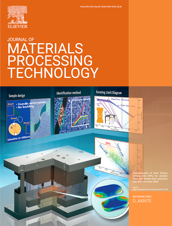
Journal of Materials Processing Technology
Journal of Materials Processing Technology 工程技术-材料科学:综合
CiteScore
12.60
自引率
4.80%
发文量
403
审稿时长
29 days
期刊介绍: The Journal of Materials Processing Technology covers the processing techniques used in manufacturing components from metals and other materials. The journal aims to publish full research papers of original, significant and rigorous work and so to contribute to increased production efficiency and improved component performance. Areas of interest to the journal include: • Casting, forming and machining • Additive processing and joining technologies • The evolution of material properties under the specific conditions met in manufacturing processes • Surface engineering when it relates specifically to a manufacturing process • Design and behavior of equipment and tools.
×
引用
GB/T 7714-2015
复制
MLA
复制
APA
复制
导出至
BibTeX EndNote RefMan NoteFirst NoteExpress
×
提示
您的信息不完整,为了账户安全,请先补充。
现在去补充
×
提示
您因"违规操作"
具体请查看互助需知
我知道了
×
提示
确定
请完成安全验证×
copy
已复制链接
快去分享给好友吧!
我知道了
右上角分享
点击右上角分享
0
联系我们:info@booksci.cn Book学术提供免费学术资源搜索服务,方便国内外学者检索中英文文献。致力于提供最便捷和优质的服务体验。 Copyright © 2023 布克学术 All rights reserved.
京ICP备2023020795号-1
ghs 京公网安备 11010802042870号
Book学术文献互助
Book学术文献互助群
群 号:604180095
Book学术官方微信