{"title":"原位畴法生长单层WS2横向同质结","authors":"Qilong Cui, Hongwei Shou, Chuanqiang Wu, Bijun Tang, Wen Zhu, Yuyang Cao, Wei Jiang, Pengjun Zhang, Ruijie Wang, Zhanfeng Liu, Shiqiang Wei, Shuangming Chen, Binghui Ge, Xiaojun Wu*, Zheng Liu* and Li Song*, ","doi":"10.1021/jacs.5c04546","DOIUrl":null,"url":null,"abstract":"<p >Two-dimensional (2D) lateral homojunctions possess unique geometries and properties distinct from those of other heterostructures, including perfect lattice matching and clean carrier diffusion channels, showing great potential in beyond-silicon nanoelectronics. However, the direct growth of 2D lateral homojunctions within the same crystal phase and layer remains challenging due to the limited choice of elements. Here, we report the epitaxy growth of semiconducting monolayer WS<sub>2</sub> lateral homojunctions by <i>in situ</i> domain engineering during chemical vapor deposition (CVD). Domain-selective defects independently modulate the electronic structures of different regions, enabling the integration of intrinsic D-/E-mode field-effect transistors within one channel. Moreover, multiple characterizations demonstrated that optimized band alignment with an ideal lattice match exists at the interface, endowing homojunctions with strong diode-like characteristics. Benefiting from the unique atomic structures, the monolayer homojunctions were used to construct homo-NMOS logic devices. The sub-1 nm-thick inverter with good rail-to-rail operation shows a peak voltage gain of 12, a dynamic delay time about 135 μs, and a peak power consumption as low as 1.3 nW. This approach paves a new way for <i>in situ</i> engineering both defect configurations and distributions within atomic layers, offering comprehensive understanding of 2D landscape as well as accelerating their potential applications.</p>","PeriodicalId":49,"journal":{"name":"Journal of the American Chemical Society","volume":"147 25","pages":"21778–21788"},"PeriodicalIF":15.6000,"publicationDate":"2025-06-13","publicationTypes":"Journal Article","fieldsOfStudy":null,"isOpenAccess":false,"openAccessPdf":"","citationCount":"0","resultStr":"{\"title\":\"Growth of Monolayer WS2 Lateral Homojunctions via In Situ Domain Engineering\",\"authors\":\"Qilong Cui, Hongwei Shou, Chuanqiang Wu, Bijun Tang, Wen Zhu, Yuyang Cao, Wei Jiang, Pengjun Zhang, Ruijie Wang, Zhanfeng Liu, Shiqiang Wei, Shuangming Chen, Binghui Ge, Xiaojun Wu*, Zheng Liu* and Li Song*, \",\"doi\":\"10.1021/jacs.5c04546\",\"DOIUrl\":null,\"url\":null,\"abstract\":\"<p >Two-dimensional (2D) lateral homojunctions possess unique geometries and properties distinct from those of other heterostructures, including perfect lattice matching and clean carrier diffusion channels, showing great potential in beyond-silicon nanoelectronics. However, the direct growth of 2D lateral homojunctions within the same crystal phase and layer remains challenging due to the limited choice of elements. Here, we report the epitaxy growth of semiconducting monolayer WS<sub>2</sub> lateral homojunctions by <i>in situ</i> domain engineering during chemical vapor deposition (CVD). Domain-selective defects independently modulate the electronic structures of different regions, enabling the integration of intrinsic D-/E-mode field-effect transistors within one channel. Moreover, multiple characterizations demonstrated that optimized band alignment with an ideal lattice match exists at the interface, endowing homojunctions with strong diode-like characteristics. Benefiting from the unique atomic structures, the monolayer homojunctions were used to construct homo-NMOS logic devices. The sub-1 nm-thick inverter with good rail-to-rail operation shows a peak voltage gain of 12, a dynamic delay time about 135 μs, and a peak power consumption as low as 1.3 nW. This approach paves a new way for <i>in situ</i> engineering both defect configurations and distributions within atomic layers, offering comprehensive understanding of 2D landscape as well as accelerating their potential applications.</p>\",\"PeriodicalId\":49,\"journal\":{\"name\":\"Journal of the American Chemical Society\",\"volume\":\"147 25\",\"pages\":\"21778–21788\"},\"PeriodicalIF\":15.6000,\"publicationDate\":\"2025-06-13\",\"publicationTypes\":\"Journal Article\",\"fieldsOfStudy\":null,\"isOpenAccess\":false,\"openAccessPdf\":\"\",\"citationCount\":\"0\",\"resultStr\":null,\"platform\":\"Semanticscholar\",\"paperid\":null,\"PeriodicalName\":\"Journal of the American Chemical Society\",\"FirstCategoryId\":\"92\",\"ListUrlMain\":\"https://pubs.acs.org/doi/10.1021/jacs.5c04546\",\"RegionNum\":1,\"RegionCategory\":\"化学\",\"ArticlePicture\":[],\"TitleCN\":null,\"AbstractTextCN\":null,\"PMCID\":null,\"EPubDate\":\"\",\"PubModel\":\"\",\"JCR\":\"Q1\",\"JCRName\":\"CHEMISTRY, MULTIDISCIPLINARY\",\"Score\":null,\"Total\":0}","platform":"Semanticscholar","paperid":null,"PeriodicalName":"Journal of the American Chemical Society","FirstCategoryId":"92","ListUrlMain":"https://pubs.acs.org/doi/10.1021/jacs.5c04546","RegionNum":1,"RegionCategory":"化学","ArticlePicture":[],"TitleCN":null,"AbstractTextCN":null,"PMCID":null,"EPubDate":"","PubModel":"","JCR":"Q1","JCRName":"CHEMISTRY, MULTIDISCIPLINARY","Score":null,"Total":0}
Growth of Monolayer WS2 Lateral Homojunctions via In Situ Domain Engineering
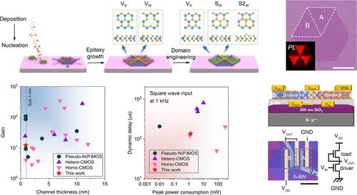
Two-dimensional (2D) lateral homojunctions possess unique geometries and properties distinct from those of other heterostructures, including perfect lattice matching and clean carrier diffusion channels, showing great potential in beyond-silicon nanoelectronics. However, the direct growth of 2D lateral homojunctions within the same crystal phase and layer remains challenging due to the limited choice of elements. Here, we report the epitaxy growth of semiconducting monolayer WS2 lateral homojunctions by in situ domain engineering during chemical vapor deposition (CVD). Domain-selective defects independently modulate the electronic structures of different regions, enabling the integration of intrinsic D-/E-mode field-effect transistors within one channel. Moreover, multiple characterizations demonstrated that optimized band alignment with an ideal lattice match exists at the interface, endowing homojunctions with strong diode-like characteristics. Benefiting from the unique atomic structures, the monolayer homojunctions were used to construct homo-NMOS logic devices. The sub-1 nm-thick inverter with good rail-to-rail operation shows a peak voltage gain of 12, a dynamic delay time about 135 μs, and a peak power consumption as low as 1.3 nW. This approach paves a new way for in situ engineering both defect configurations and distributions within atomic layers, offering comprehensive understanding of 2D landscape as well as accelerating their potential applications.
期刊介绍:
The flagship journal of the American Chemical Society, known as the Journal of the American Chemical Society (JACS), has been a prestigious publication since its establishment in 1879. It holds a preeminent position in the field of chemistry and related interdisciplinary sciences. JACS is committed to disseminating cutting-edge research papers, covering a wide range of topics, and encompasses approximately 19,000 pages of Articles, Communications, and Perspectives annually. With a weekly publication frequency, JACS plays a vital role in advancing the field of chemistry by providing essential research.

 求助内容:
求助内容: 应助结果提醒方式:


