{"title":"厘米尺度二维非层状半导体的一般“气液”合成策略","authors":"Jiahui Liu, Jiangbo Yuan, Hao Liu, Zhiyi Yuan, Baochuan Guo, Shaohui Li, Qiuhong Cui, Qun Xu and Cong Wei","doi":"10.1039/D5SC01700A","DOIUrl":null,"url":null,"abstract":"<p >Two-dimensional (2D) non-layered semiconductors have attracted tremendous research interest due to their exotic structural and electronic properties compared with their layered counterparts. However, the lack of large-scale growth methods greatly hinders their application. In this work, we have proposed a gas–liquid heterogeneous reaction strategy to suppress the diffusion of the involved reactants, resulting in the anisotropic growth of centimeter-scale 2D non-layered CdS film at the gas–liquid interface. The thickness of the 2D film can be effectively modulated in the range from 10 to 50 nm by adjusting the viscosity of the liquid solvent. A photodetector designed on the CdS film exhibits a high photoswitching (<em>I</em><small><sub>light</sub></small>/<em>I</em><small><sub>dark</sub></small>) ratio (up to 2 × 10<small><sup>3</sup></small>), high specific detectivity (∼10<small><sup>11</sup></small> Jones) and excellent stability. Moreover, centimeter-scale 2D ZnS, TiO<small><sub>2</sub></small>, SnO<small><sub>2</sub></small> and even layered MoS<small><sub>2</sub></small> were also obtained by designing corresponding reaction systems, illustrating the apparent universality of the “gas–liquid” strategy. Our results pave a novel avenue for the growth of wafer-scale 2D materials, especially non-layered ones, which will foster their potential applications in integrated optoelectronics.</p>","PeriodicalId":9909,"journal":{"name":"Chemical Science","volume":" 27","pages":" 12548-12557"},"PeriodicalIF":7.4000,"publicationDate":"2025-06-02","publicationTypes":"Journal Article","fieldsOfStudy":null,"isOpenAccess":false,"openAccessPdf":"https://pubs.rsc.org/en/content/articlepdf/2025/sc/d5sc01700a?page=search","citationCount":"0","resultStr":"{\"title\":\"A general “gas–liquid” synthesis strategy towards centimeter-scale two-dimensional non-layered semiconductors†\",\"authors\":\"Jiahui Liu, Jiangbo Yuan, Hao Liu, Zhiyi Yuan, Baochuan Guo, Shaohui Li, Qiuhong Cui, Qun Xu and Cong Wei\",\"doi\":\"10.1039/D5SC01700A\",\"DOIUrl\":null,\"url\":null,\"abstract\":\"<p >Two-dimensional (2D) non-layered semiconductors have attracted tremendous research interest due to their exotic structural and electronic properties compared with their layered counterparts. However, the lack of large-scale growth methods greatly hinders their application. In this work, we have proposed a gas–liquid heterogeneous reaction strategy to suppress the diffusion of the involved reactants, resulting in the anisotropic growth of centimeter-scale 2D non-layered CdS film at the gas–liquid interface. The thickness of the 2D film can be effectively modulated in the range from 10 to 50 nm by adjusting the viscosity of the liquid solvent. A photodetector designed on the CdS film exhibits a high photoswitching (<em>I</em><small><sub>light</sub></small>/<em>I</em><small><sub>dark</sub></small>) ratio (up to 2 × 10<small><sup>3</sup></small>), high specific detectivity (∼10<small><sup>11</sup></small> Jones) and excellent stability. Moreover, centimeter-scale 2D ZnS, TiO<small><sub>2</sub></small>, SnO<small><sub>2</sub></small> and even layered MoS<small><sub>2</sub></small> were also obtained by designing corresponding reaction systems, illustrating the apparent universality of the “gas–liquid” strategy. Our results pave a novel avenue for the growth of wafer-scale 2D materials, especially non-layered ones, which will foster their potential applications in integrated optoelectronics.</p>\",\"PeriodicalId\":9909,\"journal\":{\"name\":\"Chemical Science\",\"volume\":\" 27\",\"pages\":\" 12548-12557\"},\"PeriodicalIF\":7.4000,\"publicationDate\":\"2025-06-02\",\"publicationTypes\":\"Journal Article\",\"fieldsOfStudy\":null,\"isOpenAccess\":false,\"openAccessPdf\":\"https://pubs.rsc.org/en/content/articlepdf/2025/sc/d5sc01700a?page=search\",\"citationCount\":\"0\",\"resultStr\":null,\"platform\":\"Semanticscholar\",\"paperid\":null,\"PeriodicalName\":\"Chemical Science\",\"FirstCategoryId\":\"92\",\"ListUrlMain\":\"https://pubs.rsc.org/en/content/articlelanding/2025/sc/d5sc01700a\",\"RegionNum\":1,\"RegionCategory\":\"化学\",\"ArticlePicture\":[],\"TitleCN\":null,\"AbstractTextCN\":null,\"PMCID\":null,\"EPubDate\":\"\",\"PubModel\":\"\",\"JCR\":\"Q1\",\"JCRName\":\"CHEMISTRY, MULTIDISCIPLINARY\",\"Score\":null,\"Total\":0}","platform":"Semanticscholar","paperid":null,"PeriodicalName":"Chemical Science","FirstCategoryId":"92","ListUrlMain":"https://pubs.rsc.org/en/content/articlelanding/2025/sc/d5sc01700a","RegionNum":1,"RegionCategory":"化学","ArticlePicture":[],"TitleCN":null,"AbstractTextCN":null,"PMCID":null,"EPubDate":"","PubModel":"","JCR":"Q1","JCRName":"CHEMISTRY, MULTIDISCIPLINARY","Score":null,"Total":0}
A general “gas–liquid” synthesis strategy towards centimeter-scale two-dimensional non-layered semiconductors†
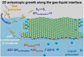
Two-dimensional (2D) non-layered semiconductors have attracted tremendous research interest due to their exotic structural and electronic properties compared with their layered counterparts. However, the lack of large-scale growth methods greatly hinders their application. In this work, we have proposed a gas–liquid heterogeneous reaction strategy to suppress the diffusion of the involved reactants, resulting in the anisotropic growth of centimeter-scale 2D non-layered CdS film at the gas–liquid interface. The thickness of the 2D film can be effectively modulated in the range from 10 to 50 nm by adjusting the viscosity of the liquid solvent. A photodetector designed on the CdS film exhibits a high photoswitching (Ilight/Idark) ratio (up to 2 × 10³), high specific detectivity (∼1011 Jones) and excellent stability. Moreover, centimeter-scale 2D ZnS, TiO2, SnO2 and even layered MoS2 were also obtained by designing corresponding reaction systems, illustrating the apparent universality of the “gas–liquid” strategy. Our results pave a novel avenue for the growth of wafer-scale 2D materials, especially non-layered ones, which will foster their potential applications in integrated optoelectronics.
期刊介绍:
Chemical Science is a journal that encompasses various disciplines within the chemical sciences. Its scope includes publishing ground-breaking research with significant implications for its respective field, as well as appealing to a wider audience in related areas. To be considered for publication, articles must showcase innovative and original advances in their field of study and be presented in a manner that is understandable to scientists from diverse backgrounds. However, the journal generally does not publish highly specialized research.
 求助内容:
求助内容: 应助结果提醒方式:


