Li-Xin Zhou, Nie-Wei Wang, Chen-Dong Jin, Hu Zhang, Peng-Lai Gong, Ru-Qian Lian, Rui-Ning Wang, Jiang-Long Wang* and Xing-Qiang Shi*,
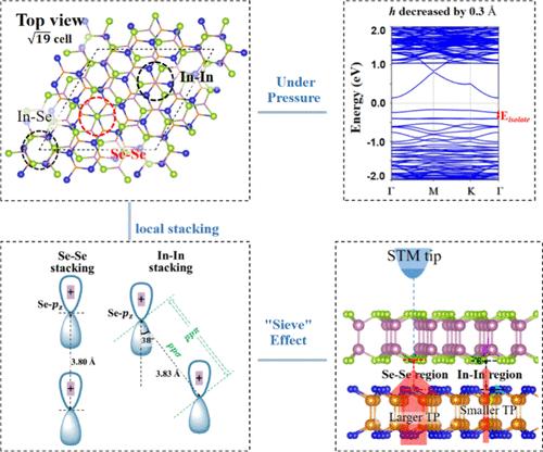
{"title":"moir<s:1>同质和异质结构的面内和面外电子及隧道特性","authors":"Li-Xin Zhou, Nie-Wei Wang, Chen-Dong Jin, Hu Zhang, Peng-Lai Gong, Ru-Qian Lian, Rui-Ning Wang, Jiang-Long Wang* and Xing-Qiang Shi*, ","doi":"10.1021/acs.jpcc.4c0750810.1021/acs.jpcc.4c07508","DOIUrl":null,"url":null,"abstract":"<p >We study the in-plane electronic and the out-of-plane tunnel properties and their correlation for moiré homo- and heterostructures. For the in-plane electronic properties, two-dimensional (2D) twisted homobilayer moiré structures often exhibit a flattening of the band edges. Using the moiré homobilayer of β-InSe, we reveal the origin of the coexistence of dispersive and flat bands in moiré structures and find that the dispersion or flatness of energy bands is related not only to the energy difference of band edges in the different local-stacking regions but also to the dispersion or flatness of the involved bands in the component monolayer and show the significance of interlayer interaction between valence and conduction bands for the formation of well-isolated flat band. Then, we uncover the effect of in-plane local potential variation on the out-of-plane tunneling properties, which is important for electronic device performance. We find that the significant variation of tunneling barriers in different local-stacking regions results in a “sieve” effect for electron tunneling across the van der Waals (vdW) gap. The “sieve” effect for the moiré heterostructure of a 3D metal/2D MoS<sub>2</sub> vdW junction explains the inverted height profile in the scanning tunneling microscopy measurement reported in the literature. Our current study focuses on the coexistence of in-plane local and nonlocal properties and the “sieve” effect for electron tunneling in different in-plane local regions, which has important implications for a broader family of moiré homo- and heterostructures of 2D semiconductor junctions and metal/2D semiconductor junctions.</p>","PeriodicalId":61,"journal":{"name":"The Journal of Physical Chemistry C","volume":"129 3","pages":"1897–1905 1897–1905"},"PeriodicalIF":3.2000,"publicationDate":"2025-01-09","publicationTypes":"Journal Article","fieldsOfStudy":null,"isOpenAccess":false,"openAccessPdf":"","citationCount":"0","resultStr":"{\"title\":\"In-Plane and Out-of-Plane Electronic and Tunnel Properties of Moiré Homo- and Heterostructures\",\"authors\":\"Li-Xin Zhou, Nie-Wei Wang, Chen-Dong Jin, Hu Zhang, Peng-Lai Gong, Ru-Qian Lian, Rui-Ning Wang, Jiang-Long Wang* and Xing-Qiang Shi*, \",\"doi\":\"10.1021/acs.jpcc.4c0750810.1021/acs.jpcc.4c07508\",\"DOIUrl\":null,\"url\":null,\"abstract\":\"<p >We study the in-plane electronic and the out-of-plane tunnel properties and their correlation for moiré homo- and heterostructures. For the in-plane electronic properties, two-dimensional (2D) twisted homobilayer moiré structures often exhibit a flattening of the band edges. Using the moiré homobilayer of β-InSe, we reveal the origin of the coexistence of dispersive and flat bands in moiré structures and find that the dispersion or flatness of energy bands is related not only to the energy difference of band edges in the different local-stacking regions but also to the dispersion or flatness of the involved bands in the component monolayer and show the significance of interlayer interaction between valence and conduction bands for the formation of well-isolated flat band. Then, we uncover the effect of in-plane local potential variation on the out-of-plane tunneling properties, which is important for electronic device performance. We find that the significant variation of tunneling barriers in different local-stacking regions results in a “sieve” effect for electron tunneling across the van der Waals (vdW) gap. The “sieve” effect for the moiré heterostructure of a 3D metal/2D MoS<sub>2</sub> vdW junction explains the inverted height profile in the scanning tunneling microscopy measurement reported in the literature. Our current study focuses on the coexistence of in-plane local and nonlocal properties and the “sieve” effect for electron tunneling in different in-plane local regions, which has important implications for a broader family of moiré homo- and heterostructures of 2D semiconductor junctions and metal/2D semiconductor junctions.</p>\",\"PeriodicalId\":61,\"journal\":{\"name\":\"The Journal of Physical Chemistry C\",\"volume\":\"129 3\",\"pages\":\"1897–1905 1897–1905\"},\"PeriodicalIF\":3.2000,\"publicationDate\":\"2025-01-09\",\"publicationTypes\":\"Journal Article\",\"fieldsOfStudy\":null,\"isOpenAccess\":false,\"openAccessPdf\":\"\",\"citationCount\":\"0\",\"resultStr\":null,\"platform\":\"Semanticscholar\",\"paperid\":null,\"PeriodicalName\":\"The Journal of Physical Chemistry C\",\"FirstCategoryId\":\"1\",\"ListUrlMain\":\"https://pubs.acs.org/doi/10.1021/acs.jpcc.4c07508\",\"RegionNum\":3,\"RegionCategory\":\"化学\",\"ArticlePicture\":[],\"TitleCN\":null,\"AbstractTextCN\":null,\"PMCID\":null,\"EPubDate\":\"\",\"PubModel\":\"\",\"JCR\":\"Q2\",\"JCRName\":\"CHEMISTRY, PHYSICAL\",\"Score\":null,\"Total\":0}","platform":"Semanticscholar","paperid":null,"PeriodicalName":"The Journal of Physical Chemistry C","FirstCategoryId":"1","ListUrlMain":"https://pubs.acs.org/doi/10.1021/acs.jpcc.4c07508","RegionNum":3,"RegionCategory":"化学","ArticlePicture":[],"TitleCN":null,"AbstractTextCN":null,"PMCID":null,"EPubDate":"","PubModel":"","JCR":"Q2","JCRName":"CHEMISTRY, PHYSICAL","Score":null,"Total":0}
In-Plane and Out-of-Plane Electronic and Tunnel Properties of Moiré Homo- and Heterostructures
We study the in-plane electronic and the out-of-plane tunnel properties and their correlation for moiré homo- and heterostructures. For the in-plane electronic properties, two-dimensional (2D) twisted homobilayer moiré structures often exhibit a flattening of the band edges. Using the moiré homobilayer of β-InSe, we reveal the origin of the coexistence of dispersive and flat bands in moiré structures and find that the dispersion or flatness of energy bands is related not only to the energy difference of band edges in the different local-stacking regions but also to the dispersion or flatness of the involved bands in the component monolayer and show the significance of interlayer interaction between valence and conduction bands for the formation of well-isolated flat band. Then, we uncover the effect of in-plane local potential variation on the out-of-plane tunneling properties, which is important for electronic device performance. We find that the significant variation of tunneling barriers in different local-stacking regions results in a “sieve” effect for electron tunneling across the van der Waals (vdW) gap. The “sieve” effect for the moiré heterostructure of a 3D metal/2D MoS2 vdW junction explains the inverted height profile in the scanning tunneling microscopy measurement reported in the literature. Our current study focuses on the coexistence of in-plane local and nonlocal properties and the “sieve” effect for electron tunneling in different in-plane local regions, which has important implications for a broader family of moiré homo- and heterostructures of 2D semiconductor junctions and metal/2D semiconductor junctions.
期刊介绍:
The Journal of Physical Chemistry A/B/C is devoted to reporting new and original experimental and theoretical basic research of interest to physical chemists, biophysical chemists, and chemical physicists.
 求助内容:
求助内容: 应助结果提醒方式:


