喷雾沉积 α-Si3N4:ZnO 薄膜的介电特性:氮化物对频率相关电容和电导曲线的影响

IF 3.4 3区 化学 Q2 CHEMISTRY, INORGANIC & NUCLEAR
Erhan İbrahimoğlu , Ahmet Demir , Fatih Çalışkan , Zafer Tatlı
{"title":"喷雾沉积 α-Si3N4:ZnO 薄膜的介电特性:氮化物对频率相关电容和电导曲线的影响","authors":"Erhan İbrahimoğlu ,&nbsp;Ahmet Demir ,&nbsp;Fatih Çalışkan ,&nbsp;Zafer Tatlı","doi":"10.1016/j.solidstatesciences.2024.107754","DOIUrl":null,"url":null,"abstract":"<div><div>The study focused on the effect of α-Si<sub>3</sub>N<sub>4</sub> doping on the electrical/dielectric properties of ZnO thin films. Both α-Si<sub>3</sub>N<sub>4</sub> doped and additive-free ZnO thin films were coated on p-Si substrates via a spray deposition method to achieve this. The electrical (current density (<em>J</em>)-voltage (<em>V</em>)) and dielectric properties (capacitance (<em>C</em>), conductance (<em>G</em>), dielectric loss (<em>tanδ</em>), reel/imaginary part of dielectric permittivity (<em>ε′</em> and <em>ε″</em>) and electric modulus (M′ and M″)) were determined for all samples by using dielectric spectroscopy (DS) method. On the other hand, scanning electron microscopy (FESEM) and energy-dispersive spectroscopy (EDS) analysis were performed to evaluate microstructure, X-ray diffraction (XRD) was used to define chemical composition and atomic-force microscopy (AFM) analysis was carried out to characterise the topology of the coating layers. The thickness/surface roughness was obtained as ∼82.5 nm/10.6 nm for undoped and ̴ 99.5 nm/10.4 nm for nitride-doped samples, respectively. The maximum capacitance value <em>(C)</em> was obtained as 275 pF at −3.0V and 200 Hz, and the optimal conductance (<em>G</em>) value was also found as 45 μS around 4.0V and 1 MHz in the nitride-doped sample. The average of α and τ values was calculated as 5.67 × 10<sup>−5</sup> s, 0.146 and 4.49 × 10<sup>−5</sup> s, 0.081 for nitride-doped and undoped ZnO, respectively. The increase in performance can be attributed to the homogeneous and almost equally-size distribution of the ZnO grain growth which is strongly controlled by α-Si<sub>3</sub>N<sub>4.</sub></div></div>","PeriodicalId":432,"journal":{"name":"Solid State Sciences","volume":"158 ","pages":"Article 107754"},"PeriodicalIF":3.4000,"publicationDate":"2024-11-07","publicationTypes":"Journal Article","fieldsOfStudy":null,"isOpenAccess":false,"openAccessPdf":"","citationCount":"0","resultStr":"{\"title\":\"The dielectric characteristics of spray deposited α-Si3N4:ZnO thin films: The nitride effect on frequency-dependent capacitance and conductance profiles\",\"authors\":\"Erhan İbrahimoğlu ,&nbsp;Ahmet Demir ,&nbsp;Fatih Çalışkan ,&nbsp;Zafer Tatlı\",\"doi\":\"10.1016/j.solidstatesciences.2024.107754\",\"DOIUrl\":null,\"url\":null,\"abstract\":\"<div><div>The study focused on the effect of α-Si<sub>3</sub>N<sub>4</sub> doping on the electrical/dielectric properties of ZnO thin films. Both α-Si<sub>3</sub>N<sub>4</sub> doped and additive-free ZnO thin films were coated on p-Si substrates via a spray deposition method to achieve this. The electrical (current density (<em>J</em>)-voltage (<em>V</em>)) and dielectric properties (capacitance (<em>C</em>), conductance (<em>G</em>), dielectric loss (<em>tanδ</em>), reel/imaginary part of dielectric permittivity (<em>ε′</em> and <em>ε″</em>) and electric modulus (M′ and M″)) were determined for all samples by using dielectric spectroscopy (DS) method. On the other hand, scanning electron microscopy (FESEM) and energy-dispersive spectroscopy (EDS) analysis were performed to evaluate microstructure, X-ray diffraction (XRD) was used to define chemical composition and atomic-force microscopy (AFM) analysis was carried out to characterise the topology of the coating layers. The thickness/surface roughness was obtained as ∼82.5 nm/10.6 nm for undoped and ̴ 99.5 nm/10.4 nm for nitride-doped samples, respectively. The maximum capacitance value <em>(C)</em> was obtained as 275 pF at −3.0V and 200 Hz, and the optimal conductance (<em>G</em>) value was also found as 45 μS around 4.0V and 1 MHz in the nitride-doped sample. The average of α and τ values was calculated as 5.67 × 10<sup>−5</sup> s, 0.146 and 4.49 × 10<sup>−5</sup> s, 0.081 for nitride-doped and undoped ZnO, respectively. The increase in performance can be attributed to the homogeneous and almost equally-size distribution of the ZnO grain growth which is strongly controlled by α-Si<sub>3</sub>N<sub>4.</sub></div></div>\",\"PeriodicalId\":432,\"journal\":{\"name\":\"Solid State Sciences\",\"volume\":\"158 \",\"pages\":\"Article 107754\"},\"PeriodicalIF\":3.4000,\"publicationDate\":\"2024-11-07\",\"publicationTypes\":\"Journal Article\",\"fieldsOfStudy\":null,\"isOpenAccess\":false,\"openAccessPdf\":\"\",\"citationCount\":\"0\",\"resultStr\":null,\"platform\":\"Semanticscholar\",\"paperid\":null,\"PeriodicalName\":\"Solid State Sciences\",\"FirstCategoryId\":\"92\",\"ListUrlMain\":\"https://www.sciencedirect.com/science/article/pii/S1293255824003194\",\"RegionNum\":3,\"RegionCategory\":\"化学\",\"ArticlePicture\":[],\"TitleCN\":null,\"AbstractTextCN\":null,\"PMCID\":null,\"EPubDate\":\"\",\"PubModel\":\"\",\"JCR\":\"Q2\",\"JCRName\":\"CHEMISTRY, INORGANIC & NUCLEAR\",\"Score\":null,\"Total\":0}","platform":"Semanticscholar","paperid":null,"PeriodicalName":"Solid State Sciences","FirstCategoryId":"92","ListUrlMain":"https://www.sciencedirect.com/science/article/pii/S1293255824003194","RegionNum":3,"RegionCategory":"化学","ArticlePicture":[],"TitleCN":null,"AbstractTextCN":null,"PMCID":null,"EPubDate":"","PubModel":"","JCR":"Q2","JCRName":"CHEMISTRY, INORGANIC & NUCLEAR","Score":null,"Total":0}
引用次数: 0

摘要

研究重点是掺杂α-Si3N4对氧化锌薄膜电学/介电性能的影响。为此,研究人员采用喷雾沉积法在对硅衬底上镀上了掺杂了 α-Si3N4 和无添加剂的氧化锌薄膜。所有样品的电性能(电流密度(J)-电压(V))和介电性能(电容(C)、电导(G)、介电损耗(tanδ)、介电常数的卷积/虚部(ε′和ε″)以及电模量(M′和M″))都是通过介电光谱法(DS)测定的。另一方面,扫描电子显微镜(FESEM)和能量色散光谱(EDS)分析用于评估微观结构,X 射线衍射(XRD)用于确定化学成分,原子力显微镜(AFM)分析用于表征涂层层的拓扑结构。未掺杂样品的厚度/表面粗糙度分别为 ∼82.5 nm/10.6 nm,掺氮化物样品的厚度/表面粗糙度分别为 ̴ 99.5 nm/10.4 nm。掺氮样品在 -3.0V 和 200 Hz 时的最大电容值 (C) 为 275 pF,在 4.0V 和 1 MHz 时的最佳电导 (G) 值为 45 μS。经计算,掺氮和未掺氮氧化物的 α 和 τ 值平均值分别为 5.67 × 10⁻⁵ s, 0.146 和 4.49 × 10⁻⁵ s, 0.081。性能的提高可归因于 ZnO 晶粒生长的均匀性和几乎相同大小的分布,而这在α-Si3N4 的强烈控制下得以实现。
本文章由计算机程序翻译,如有差异,请以英文原文为准。

The dielectric characteristics of spray deposited α-Si3N4:ZnO thin films: The nitride effect on frequency-dependent capacitance and conductance profiles

The dielectric characteristics of spray deposited α-Si3N4:ZnO thin films: The nitride effect on frequency-dependent capacitance and conductance profiles
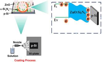
The study focused on the effect of α-Si3N4 doping on the electrical/dielectric properties of ZnO thin films. Both α-Si3N4 doped and additive-free ZnO thin films were coated on p-Si substrates via a spray deposition method to achieve this. The electrical (current density (J)-voltage (V)) and dielectric properties (capacitance (C), conductance (G), dielectric loss (tanδ), reel/imaginary part of dielectric permittivity (ε′ and ε″) and electric modulus (M′ and M″)) were determined for all samples by using dielectric spectroscopy (DS) method. On the other hand, scanning electron microscopy (FESEM) and energy-dispersive spectroscopy (EDS) analysis were performed to evaluate microstructure, X-ray diffraction (XRD) was used to define chemical composition and atomic-force microscopy (AFM) analysis was carried out to characterise the topology of the coating layers. The thickness/surface roughness was obtained as ∼82.5 nm/10.6 nm for undoped and ̴ 99.5 nm/10.4 nm for nitride-doped samples, respectively. The maximum capacitance value (C) was obtained as 275 pF at −3.0V and 200 Hz, and the optimal conductance (G) value was also found as 45 μS around 4.0V and 1 MHz in the nitride-doped sample. The average of α and τ values was calculated as 5.67 × 10−5 s, 0.146 and 4.49 × 10−5 s, 0.081 for nitride-doped and undoped ZnO, respectively. The increase in performance can be attributed to the homogeneous and almost equally-size distribution of the ZnO grain growth which is strongly controlled by α-Si3N4.
求助全文
通过发布文献求助,成功后即可免费获取论文全文。 去求助
来源期刊
Solid State Sciences
Solid State Sciences 化学-无机化学与核化学
CiteScore
6.60
自引率
2.90%
发文量
214
审稿时长
27 days
期刊介绍: Solid State Sciences is the journal for researchers from the broad solid state chemistry and physics community. It publishes key articles on all aspects of solid state synthesis, structure-property relationships, theory and functionalities, in relation with experiments. Key topics for stand-alone papers and special issues: -Novel ways of synthesis, inorganic functional materials, including porous and glassy materials, hybrid organic-inorganic compounds and nanomaterials -Physical properties, emphasizing but not limited to the electrical, magnetical and optical features -Materials related to information technology and energy and environmental sciences. The journal publishes feature articles from experts in the field upon invitation. Solid State Sciences - your gateway to energy-related materials.
×
引用
GB/T 7714-2015
复制
MLA
复制
APA
复制
导出至
BibTeX EndNote RefMan NoteFirst NoteExpress
×
提示
您的信息不完整,为了账户安全,请先补充。
现在去补充
×
提示
您因"违规操作"
具体请查看互助需知
我知道了
×
提示
确定
请完成安全验证×
copy
已复制链接
快去分享给好友吧!
我知道了
右上角分享
点击右上角分享
0
联系我们:info@booksci.cn Book学术提供免费学术资源搜索服务,方便国内外学者检索中英文文献。致力于提供最便捷和优质的服务体验。 Copyright © 2023 布克学术 All rights reserved.
京ICP备2023020795号-1
ghs 京公网安备 11010802042870号
Book学术文献互助
Book学术文献互助群
群 号:481959085
Book学术官方微信