{"title":"利用第一原理方法分析基于掺杂之字形石墨烯纳米带的实用电子应用器件的性能","authors":"Hammadur Rub Ansari , M. Nizamuddin , Samrah Manzoor , Prabhash Mishra","doi":"10.1016/j.commatsci.2024.113464","DOIUrl":null,"url":null,"abstract":"<div><div>The ongoing reduction in the size of electronic devices, interconnect delays have emerged as an important constraint in the overall performance of chips. The time it takes for signals to travel over the interconnecting wires is the cause of these delays, which today frequently exceed the intrinsic delays that are present within the integrated circuits (ICs) themselves. The rate at which current chips operate and their overall efficiency are both significantly influenced by this trend. This research investigates the electrical and electronic properties of a device constructed from doped graphene nanoribbons. The device is analyzed under conditions of minimal applied bias or electric field. It features a channel consisting of a minimal unit cell from a zigzag nanoribbon, situated between two zigzag graphene nanoribbons (ZGNR) which function as the electrodes on the left and right sides. The doping process improves the thermodynamic and structural stability of the device, achieving notably low values for total energy, formation energy, and binding energy. By incorporating nitrogen and boron atoms into specific interstitial sites within the ZGNR, the study aims to enhance understanding of the electronic transport mechanisms involving these dopant atoms and the lattice of the ZGNR. This research explores key semiconductor characteristics of the doped ZGNR-based device, such as negative differential resistance (NDR), peak-to-valley ratio (PVR), and rectification ratio (RR), which are crucial for various electronic applications, including switches, logic circuits, memory storage, amplifiers, and negative resistance oscillators. The device demonstrates a peak-to-valley ratio (PVR) of 92 and a rectification ratio (RR) of 149. Additionally, the device exhibits high dielectric energy storage capacity, with a maximum static dielectric constant of 14.7 and substantial low-energy absorption when nitrogen atoms are incorporated into the electrode region. This suggests potential applications in nanoelectronics and as a dielectric energy storage device operating at low applied bias voltages.</div></div>","PeriodicalId":10650,"journal":{"name":"Computational Materials Science","volume":"247 ","pages":"Article 113464"},"PeriodicalIF":3.1000,"publicationDate":"2024-11-09","publicationTypes":"Journal Article","fieldsOfStudy":null,"isOpenAccess":false,"openAccessPdf":"","citationCount":"0","resultStr":"{\"title\":\"Performance analysis of doped zigzag graphene nanoribbon-based device for practical electronic applications using first principle approach\",\"authors\":\"Hammadur Rub Ansari , M. Nizamuddin , Samrah Manzoor , Prabhash Mishra\",\"doi\":\"10.1016/j.commatsci.2024.113464\",\"DOIUrl\":null,\"url\":null,\"abstract\":\"<div><div>The ongoing reduction in the size of electronic devices, interconnect delays have emerged as an important constraint in the overall performance of chips. The time it takes for signals to travel over the interconnecting wires is the cause of these delays, which today frequently exceed the intrinsic delays that are present within the integrated circuits (ICs) themselves. The rate at which current chips operate and their overall efficiency are both significantly influenced by this trend. This research investigates the electrical and electronic properties of a device constructed from doped graphene nanoribbons. The device is analyzed under conditions of minimal applied bias or electric field. It features a channel consisting of a minimal unit cell from a zigzag nanoribbon, situated between two zigzag graphene nanoribbons (ZGNR) which function as the electrodes on the left and right sides. The doping process improves the thermodynamic and structural stability of the device, achieving notably low values for total energy, formation energy, and binding energy. By incorporating nitrogen and boron atoms into specific interstitial sites within the ZGNR, the study aims to enhance understanding of the electronic transport mechanisms involving these dopant atoms and the lattice of the ZGNR. This research explores key semiconductor characteristics of the doped ZGNR-based device, such as negative differential resistance (NDR), peak-to-valley ratio (PVR), and rectification ratio (RR), which are crucial for various electronic applications, including switches, logic circuits, memory storage, amplifiers, and negative resistance oscillators. The device demonstrates a peak-to-valley ratio (PVR) of 92 and a rectification ratio (RR) of 149. Additionally, the device exhibits high dielectric energy storage capacity, with a maximum static dielectric constant of 14.7 and substantial low-energy absorption when nitrogen atoms are incorporated into the electrode region. This suggests potential applications in nanoelectronics and as a dielectric energy storage device operating at low applied bias voltages.</div></div>\",\"PeriodicalId\":10650,\"journal\":{\"name\":\"Computational Materials Science\",\"volume\":\"247 \",\"pages\":\"Article 113464\"},\"PeriodicalIF\":3.1000,\"publicationDate\":\"2024-11-09\",\"publicationTypes\":\"Journal Article\",\"fieldsOfStudy\":null,\"isOpenAccess\":false,\"openAccessPdf\":\"\",\"citationCount\":\"0\",\"resultStr\":null,\"platform\":\"Semanticscholar\",\"paperid\":null,\"PeriodicalName\":\"Computational Materials Science\",\"FirstCategoryId\":\"88\",\"ListUrlMain\":\"https://www.sciencedirect.com/science/article/pii/S0927025624006852\",\"RegionNum\":3,\"RegionCategory\":\"材料科学\",\"ArticlePicture\":[],\"TitleCN\":null,\"AbstractTextCN\":null,\"PMCID\":null,\"EPubDate\":\"\",\"PubModel\":\"\",\"JCR\":\"Q2\",\"JCRName\":\"MATERIALS SCIENCE, MULTIDISCIPLINARY\",\"Score\":null,\"Total\":0}","platform":"Semanticscholar","paperid":null,"PeriodicalName":"Computational Materials Science","FirstCategoryId":"88","ListUrlMain":"https://www.sciencedirect.com/science/article/pii/S0927025624006852","RegionNum":3,"RegionCategory":"材料科学","ArticlePicture":[],"TitleCN":null,"AbstractTextCN":null,"PMCID":null,"EPubDate":"","PubModel":"","JCR":"Q2","JCRName":"MATERIALS SCIENCE, MULTIDISCIPLINARY","Score":null,"Total":0}
Performance analysis of doped zigzag graphene nanoribbon-based device for practical electronic applications using first principle approach
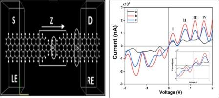
The ongoing reduction in the size of electronic devices, interconnect delays have emerged as an important constraint in the overall performance of chips. The time it takes for signals to travel over the interconnecting wires is the cause of these delays, which today frequently exceed the intrinsic delays that are present within the integrated circuits (ICs) themselves. The rate at which current chips operate and their overall efficiency are both significantly influenced by this trend. This research investigates the electrical and electronic properties of a device constructed from doped graphene nanoribbons. The device is analyzed under conditions of minimal applied bias or electric field. It features a channel consisting of a minimal unit cell from a zigzag nanoribbon, situated between two zigzag graphene nanoribbons (ZGNR) which function as the electrodes on the left and right sides. The doping process improves the thermodynamic and structural stability of the device, achieving notably low values for total energy, formation energy, and binding energy. By incorporating nitrogen and boron atoms into specific interstitial sites within the ZGNR, the study aims to enhance understanding of the electronic transport mechanisms involving these dopant atoms and the lattice of the ZGNR. This research explores key semiconductor characteristics of the doped ZGNR-based device, such as negative differential resistance (NDR), peak-to-valley ratio (PVR), and rectification ratio (RR), which are crucial for various electronic applications, including switches, logic circuits, memory storage, amplifiers, and negative resistance oscillators. The device demonstrates a peak-to-valley ratio (PVR) of 92 and a rectification ratio (RR) of 149. Additionally, the device exhibits high dielectric energy storage capacity, with a maximum static dielectric constant of 14.7 and substantial low-energy absorption when nitrogen atoms are incorporated into the electrode region. This suggests potential applications in nanoelectronics and as a dielectric energy storage device operating at low applied bias voltages.
期刊介绍:
The goal of Computational Materials Science is to report on results that provide new or unique insights into, or significantly expand our understanding of, the properties of materials or phenomena associated with their design, synthesis, processing, characterization, and utilization. To be relevant to the journal, the results should be applied or applicable to specific material systems that are discussed within the submission.