GaN(0001) 薄膜/蓝宝石(0001)上 1 至 3 单层外延 WS2 和 MoS2 薄膜的面内和面外畴取向分散

IF 2.9 3区 物理与天体物理 Q3 NANOSCIENCE & NANOTECHNOLOGY
Shalini Kumari , Neha Dhull , Weichang Lin , Zonghuan Lu , Joan Redwing , Toh-Ming Lu , Gwo-Ching Wang
{"title":"GaN(0001) 薄膜/蓝宝石(0001)上 1 至 3 单层外延 WS2 和 MoS2 薄膜的面内和面外畴取向分散","authors":"Shalini Kumari ,&nbsp;Neha Dhull ,&nbsp;Weichang Lin ,&nbsp;Zonghuan Lu ,&nbsp;Joan Redwing ,&nbsp;Toh-Ming Lu ,&nbsp;Gwo-Ching Wang","doi":"10.1016/j.physe.2024.116117","DOIUrl":null,"url":null,"abstract":"<div><div>Transition-metal dichalcogenides and their heterostructures have attractive potential applications in electronics and optoelectronics. Wafer scale 1 to 3 monolayers WS<sub>2</sub> and MoS<sub>2</sub> ultrathin films on GaN/sapphire substrates were grown by metal organic chemical vapor deposition. Azimuthal reflection high-energy electron diffraction (ARHEED) was used to characterize the long-range order of these TMDC ultrathin films. The RHEED patterns of WS<sub>2</sub> and MoS<sub>2</sub> show stripes and arcs but the MoS<sub>2</sub> on GaN shows sharp spots in addition to stripes and arcs. The 2D map constructed from ARHEED patterns shows that WS<sub>2</sub> is epitaxial and has an in-plane domain orientation dispersion. For the MoS<sub>2</sub> on GaN/sapphire substrate, the 2D map shows concentric continuous rings for each diffraction order of MoS<sub>2</sub> and GaN indicating that the in-plane MoS<sub>2</sub> domain orientation and GaN nanocrystals are random. The out-of-plane orientation dispersion of MoS<sub>2</sub> on the GaN substrate is larger than that of WS<sub>2</sub> on the GaN substrate. The observations of stripes, arcs, and spots from RHEED patterns and the 2D maps reveal the deviation of ultrathin epitaxial films from its perfect epitaxy, especially the TMDC domain orientation dispersion over a large area. These rich findings from 2D maps broaden the application of ARHEED in more than one monolayer thick 2D materials.</div></div>","PeriodicalId":20181,"journal":{"name":"Physica E-low-dimensional Systems & Nanostructures","volume":"165 ","pages":"Article 116117"},"PeriodicalIF":2.9000,"publicationDate":"2024-10-01","publicationTypes":"Journal Article","fieldsOfStudy":null,"isOpenAccess":false,"openAccessPdf":"","citationCount":"0","resultStr":"{\"title\":\"In-plane and out-of-plane domain orientation dispersions in 1 to 3 monolayers epitaxial WS2 and MoS2 films on GaN(0001) film/sapphire(0001)\",\"authors\":\"Shalini Kumari ,&nbsp;Neha Dhull ,&nbsp;Weichang Lin ,&nbsp;Zonghuan Lu ,&nbsp;Joan Redwing ,&nbsp;Toh-Ming Lu ,&nbsp;Gwo-Ching Wang\",\"doi\":\"10.1016/j.physe.2024.116117\",\"DOIUrl\":null,\"url\":null,\"abstract\":\"<div><div>Transition-metal dichalcogenides and their heterostructures have attractive potential applications in electronics and optoelectronics. Wafer scale 1 to 3 monolayers WS<sub>2</sub> and MoS<sub>2</sub> ultrathin films on GaN/sapphire substrates were grown by metal organic chemical vapor deposition. Azimuthal reflection high-energy electron diffraction (ARHEED) was used to characterize the long-range order of these TMDC ultrathin films. The RHEED patterns of WS<sub>2</sub> and MoS<sub>2</sub> show stripes and arcs but the MoS<sub>2</sub> on GaN shows sharp spots in addition to stripes and arcs. The 2D map constructed from ARHEED patterns shows that WS<sub>2</sub> is epitaxial and has an in-plane domain orientation dispersion. For the MoS<sub>2</sub> on GaN/sapphire substrate, the 2D map shows concentric continuous rings for each diffraction order of MoS<sub>2</sub> and GaN indicating that the in-plane MoS<sub>2</sub> domain orientation and GaN nanocrystals are random. The out-of-plane orientation dispersion of MoS<sub>2</sub> on the GaN substrate is larger than that of WS<sub>2</sub> on the GaN substrate. The observations of stripes, arcs, and spots from RHEED patterns and the 2D maps reveal the deviation of ultrathin epitaxial films from its perfect epitaxy, especially the TMDC domain orientation dispersion over a large area. These rich findings from 2D maps broaden the application of ARHEED in more than one monolayer thick 2D materials.</div></div>\",\"PeriodicalId\":20181,\"journal\":{\"name\":\"Physica E-low-dimensional Systems & Nanostructures\",\"volume\":\"165 \",\"pages\":\"Article 116117\"},\"PeriodicalIF\":2.9000,\"publicationDate\":\"2024-10-01\",\"publicationTypes\":\"Journal Article\",\"fieldsOfStudy\":null,\"isOpenAccess\":false,\"openAccessPdf\":\"\",\"citationCount\":\"0\",\"resultStr\":null,\"platform\":\"Semanticscholar\",\"paperid\":null,\"PeriodicalName\":\"Physica E-low-dimensional Systems & Nanostructures\",\"FirstCategoryId\":\"101\",\"ListUrlMain\":\"https://www.sciencedirect.com/science/article/pii/S1386947724002212\",\"RegionNum\":3,\"RegionCategory\":\"物理与天体物理\",\"ArticlePicture\":[],\"TitleCN\":null,\"AbstractTextCN\":null,\"PMCID\":null,\"EPubDate\":\"\",\"PubModel\":\"\",\"JCR\":\"Q3\",\"JCRName\":\"NANOSCIENCE & NANOTECHNOLOGY\",\"Score\":null,\"Total\":0}","platform":"Semanticscholar","paperid":null,"PeriodicalName":"Physica E-low-dimensional Systems & Nanostructures","FirstCategoryId":"101","ListUrlMain":"https://www.sciencedirect.com/science/article/pii/S1386947724002212","RegionNum":3,"RegionCategory":"物理与天体物理","ArticlePicture":[],"TitleCN":null,"AbstractTextCN":null,"PMCID":null,"EPubDate":"","PubModel":"","JCR":"Q3","JCRName":"NANOSCIENCE & NANOTECHNOLOGY","Score":null,"Total":0}
引用次数: 0

摘要

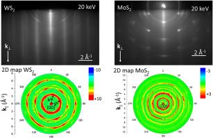
过渡金属二卤化物及其异质结构在电子学和光电子学领域有着极具吸引力的潜在应用。通过金属有机化学气相沉积法在氮化镓/蓝宝石衬底上生长了晶圆级 1 至 3 单层 WS2 和 MoS2 超薄薄膜。方位反射高能电子衍射(ARHEED)用于表征这些 TMDC 超薄薄膜的长程有序性。WS2 和 MoS2 的方位反射高能电子衍射图显示出条纹和弧线,但 GaN 上的 MoS2 除条纹和弧线外,还显示出尖锐的斑点。根据 ARHEED 图形绘制的二维图显示,WS2 是外延的,具有面内畴取向分散性。对于在氮化镓/蓝宝石衬底上的 MoS2,二维图显示出 MoS2 和 GaN 的每个衍射阶的同心连续环,表明 MoS2 的面内畴取向和 GaN 纳米晶体是随机的。在氮化镓衬底上,MoS2 的面外取向分散度大于在氮化镓衬底上的 WS2。从 RHEED 图形和二维地图中观察到的条纹、弧线和斑点揭示了超薄外延薄膜与完美外延的偏差,尤其是大面积的 TMDC 结构域取向分散。二维地图的这些丰富发现拓宽了 ARHEED 在单层厚二维材料以外的应用。
本文章由计算机程序翻译,如有差异,请以英文原文为准。

In-plane and out-of-plane domain orientation dispersions in 1 to 3 monolayers epitaxial WS2 and MoS2 films on GaN(0001) film/sapphire(0001)

In-plane and out-of-plane domain orientation dispersions in 1 to 3 monolayers epitaxial WS2 and MoS2 films on GaN(0001) film/sapphire(0001)
Transition-metal dichalcogenides and their heterostructures have attractive potential applications in electronics and optoelectronics. Wafer scale 1 to 3 monolayers WS2 and MoS2 ultrathin films on GaN/sapphire substrates were grown by metal organic chemical vapor deposition. Azimuthal reflection high-energy electron diffraction (ARHEED) was used to characterize the long-range order of these TMDC ultrathin films. The RHEED patterns of WS2 and MoS2 show stripes and arcs but the MoS2 on GaN shows sharp spots in addition to stripes and arcs. The 2D map constructed from ARHEED patterns shows that WS2 is epitaxial and has an in-plane domain orientation dispersion. For the MoS2 on GaN/sapphire substrate, the 2D map shows concentric continuous rings for each diffraction order of MoS2 and GaN indicating that the in-plane MoS2 domain orientation and GaN nanocrystals are random. The out-of-plane orientation dispersion of MoS2 on the GaN substrate is larger than that of WS2 on the GaN substrate. The observations of stripes, arcs, and spots from RHEED patterns and the 2D maps reveal the deviation of ultrathin epitaxial films from its perfect epitaxy, especially the TMDC domain orientation dispersion over a large area. These rich findings from 2D maps broaden the application of ARHEED in more than one monolayer thick 2D materials.
求助全文
通过发布文献求助,成功后即可免费获取论文全文。 去求助
来源期刊
CiteScore
7.30
自引率
6.10%
发文量
356
审稿时长
65 days
期刊介绍: Physica E: Low-dimensional systems and nanostructures contains papers and invited review articles on the fundamental and applied aspects of physics in low-dimensional electron systems, in semiconductor heterostructures, oxide interfaces, quantum wells and superlattices, quantum wires and dots, novel quantum states of matter such as topological insulators, and Weyl semimetals. Both theoretical and experimental contributions are invited. Topics suitable for publication in this journal include spin related phenomena, optical and transport properties, many-body effects, integer and fractional quantum Hall effects, quantum spin Hall effect, single electron effects and devices, Majorana fermions, and other novel phenomena. Keywords: • topological insulators/superconductors, majorana fermions, Wyel semimetals; • quantum and neuromorphic computing/quantum information physics and devices based on low dimensional systems; • layered superconductivity, low dimensional systems with superconducting proximity effect; • 2D materials such as transition metal dichalcogenides; • oxide heterostructures including ZnO, SrTiO3 etc; • carbon nanostructures (graphene, carbon nanotubes, diamond NV center, etc.) • quantum wells and superlattices; • quantum Hall effect, quantum spin Hall effect, quantum anomalous Hall effect; • optical- and phonons-related phenomena; • magnetic-semiconductor structures; • charge/spin-, magnon-, skyrmion-, Cooper pair- and majorana fermion- transport and tunneling; • ultra-fast nonlinear optical phenomena; • novel devices and applications (such as high performance sensor, solar cell, etc); • novel growth and fabrication techniques for nanostructures
×
引用
GB/T 7714-2015
复制
MLA
复制
APA
复制
导出至
BibTeX EndNote RefMan NoteFirst NoteExpress
×
提示
您的信息不完整,为了账户安全,请先补充。
现在去补充
×
提示
您因"违规操作"
具体请查看互助需知
我知道了
×
提示
确定
请完成安全验证×
copy
已复制链接
快去分享给好友吧!
我知道了
右上角分享
点击右上角分享
0
联系我们:info@booksci.cn Book学术提供免费学术资源搜索服务,方便国内外学者检索中英文文献。致力于提供最便捷和优质的服务体验。 Copyright © 2023 布克学术 All rights reserved.
京ICP备2023020795号-1
ghs 京公网安备 11010802042870号
Book学术文献互助
Book学术文献互助群
群 号:481959085
Book学术官方微信