Md Nahiduzzaman Nahid , Md Salman Shah , Hayati Mamur , Rakib Hosen , Mohammad Ruhul Amin Bhuiyan
{"title":"利用 SCAPS-1D 软件优化无铅 CH3NH3SnI3 包晶太阳能电池","authors":"Md Nahiduzzaman Nahid , Md Salman Shah , Hayati Mamur , Rakib Hosen , Mohammad Ruhul Amin Bhuiyan","doi":"10.1016/j.cinorg.2024.100069","DOIUrl":null,"url":null,"abstract":"<div><div>The lead-free CH<sub>3</sub>NH<sub>3</sub>SnI<sub>3</sub> perovskite is essential for absorbing light in perovskite solar cells (PSCs). In a photovoltaic (PV) device setup of FTO/STO/CH<sub>3</sub>NH<sub>3</sub>SnI<sub>3</sub>/Spiro-OMeTAD/Au, it demonstrates excellent PV performance. This device includes sulfur-doped tin oxide (STO) for the layer of electron transport (ETL), CH<sub>3</sub>NH<sub>3</sub>SnI<sub>3</sub> as the absorber, and the hole transport layer (HTL) is Spiro-OMeTAD. The upper and back contacts consist of fluorine-doped tin oxide (FTO) and gold (Au), connecting these layers. Several parameters were estimated using the Solar Cell Capacitance Simulator (SCAPS-1D) program, including the thickness, acceptor and donor densities, series and shunt resistances, and temperature. The absorber, HTL, ETL, and FTO thicknesses were set at 1000 nm, 100 nm, 150 nm, and 50 nm, respectively, to find the perfect configuration. Densities of acceptors and donors were maintained at 10<sup>19</sup> cm<sup>−3</sup>, 2.0 × 10<sup>19</sup> cm<sup>−3</sup>, 2.0 × 10<sup>18</sup> cm<sup>−3</sup>, and 10<sup>18</sup> cm<sup>−3</sup> for the absorber, HTL, ETL, and FTO, respectively, at an operating temperature of 300K. The device configuration exhibited reduced series resistance and increased shunt resistance, optimized with a back contact metal of Au. The idealized model demonstrated significant PV execution characteristics, including 1.117 V for open-circuit voltage (V<sub>OC</sub>), 28.88 mA/cm<sup>2</sup> for short-circuit current density (J<sub>SC</sub>), 88.47 % for fill factor (FF), and 28.55 % for power conversion efficiency (PCE) under the AM1.5G spectrum. Additionally, the device displayed an average quantum efficiency (QE) of approximately 88.30 % at visible light wavelengths.</div></div>","PeriodicalId":100233,"journal":{"name":"Chemistry of Inorganic Materials","volume":"4 ","pages":"Article 100069"},"PeriodicalIF":0.0000,"publicationDate":"2024-09-24","publicationTypes":"Journal Article","fieldsOfStudy":null,"isOpenAccess":false,"openAccessPdf":"","citationCount":"0","resultStr":"{\"title\":\"Optimizing lead-free CH3NH3SnI3 perovskite solar cells by using SCAPS-1D software\",\"authors\":\"Md Nahiduzzaman Nahid , Md Salman Shah , Hayati Mamur , Rakib Hosen , Mohammad Ruhul Amin Bhuiyan\",\"doi\":\"10.1016/j.cinorg.2024.100069\",\"DOIUrl\":null,\"url\":null,\"abstract\":\"<div><div>The lead-free CH<sub>3</sub>NH<sub>3</sub>SnI<sub>3</sub> perovskite is essential for absorbing light in perovskite solar cells (PSCs). In a photovoltaic (PV) device setup of FTO/STO/CH<sub>3</sub>NH<sub>3</sub>SnI<sub>3</sub>/Spiro-OMeTAD/Au, it demonstrates excellent PV performance. This device includes sulfur-doped tin oxide (STO) for the layer of electron transport (ETL), CH<sub>3</sub>NH<sub>3</sub>SnI<sub>3</sub> as the absorber, and the hole transport layer (HTL) is Spiro-OMeTAD. The upper and back contacts consist of fluorine-doped tin oxide (FTO) and gold (Au), connecting these layers. Several parameters were estimated using the Solar Cell Capacitance Simulator (SCAPS-1D) program, including the thickness, acceptor and donor densities, series and shunt resistances, and temperature. The absorber, HTL, ETL, and FTO thicknesses were set at 1000 nm, 100 nm, 150 nm, and 50 nm, respectively, to find the perfect configuration. Densities of acceptors and donors were maintained at 10<sup>19</sup> cm<sup>−3</sup>, 2.0 × 10<sup>19</sup> cm<sup>−3</sup>, 2.0 × 10<sup>18</sup> cm<sup>−3</sup>, and 10<sup>18</sup> cm<sup>−3</sup> for the absorber, HTL, ETL, and FTO, respectively, at an operating temperature of 300K. The device configuration exhibited reduced series resistance and increased shunt resistance, optimized with a back contact metal of Au. The idealized model demonstrated significant PV execution characteristics, including 1.117 V for open-circuit voltage (V<sub>OC</sub>), 28.88 mA/cm<sup>2</sup> for short-circuit current density (J<sub>SC</sub>), 88.47 % for fill factor (FF), and 28.55 % for power conversion efficiency (PCE) under the AM1.5G spectrum. Additionally, the device displayed an average quantum efficiency (QE) of approximately 88.30 % at visible light wavelengths.</div></div>\",\"PeriodicalId\":100233,\"journal\":{\"name\":\"Chemistry of Inorganic Materials\",\"volume\":\"4 \",\"pages\":\"Article 100069\"},\"PeriodicalIF\":0.0000,\"publicationDate\":\"2024-09-24\",\"publicationTypes\":\"Journal Article\",\"fieldsOfStudy\":null,\"isOpenAccess\":false,\"openAccessPdf\":\"\",\"citationCount\":\"0\",\"resultStr\":null,\"platform\":\"Semanticscholar\",\"paperid\":null,\"PeriodicalName\":\"Chemistry of Inorganic Materials\",\"FirstCategoryId\":\"1085\",\"ListUrlMain\":\"https://www.sciencedirect.com/science/article/pii/S2949746924000375\",\"RegionNum\":0,\"RegionCategory\":null,\"ArticlePicture\":[],\"TitleCN\":null,\"AbstractTextCN\":null,\"PMCID\":null,\"EPubDate\":\"\",\"PubModel\":\"\",\"JCR\":\"\",\"JCRName\":\"\",\"Score\":null,\"Total\":0}","platform":"Semanticscholar","paperid":null,"PeriodicalName":"Chemistry of Inorganic Materials","FirstCategoryId":"1085","ListUrlMain":"https://www.sciencedirect.com/science/article/pii/S2949746924000375","RegionNum":0,"RegionCategory":null,"ArticlePicture":[],"TitleCN":null,"AbstractTextCN":null,"PMCID":null,"EPubDate":"","PubModel":"","JCR":"","JCRName":"","Score":null,"Total":0}
Optimizing lead-free CH3NH3SnI3 perovskite solar cells by using SCAPS-1D software
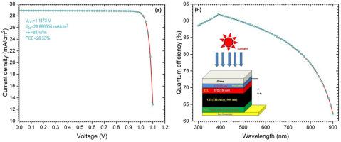
The lead-free CH3NH3SnI3 perovskite is essential for absorbing light in perovskite solar cells (PSCs). In a photovoltaic (PV) device setup of FTO/STO/CH3NH3SnI3/Spiro-OMeTAD/Au, it demonstrates excellent PV performance. This device includes sulfur-doped tin oxide (STO) for the layer of electron transport (ETL), CH3NH3SnI3 as the absorber, and the hole transport layer (HTL) is Spiro-OMeTAD. The upper and back contacts consist of fluorine-doped tin oxide (FTO) and gold (Au), connecting these layers. Several parameters were estimated using the Solar Cell Capacitance Simulator (SCAPS-1D) program, including the thickness, acceptor and donor densities, series and shunt resistances, and temperature. The absorber, HTL, ETL, and FTO thicknesses were set at 1000 nm, 100 nm, 150 nm, and 50 nm, respectively, to find the perfect configuration. Densities of acceptors and donors were maintained at 1019 cm−3, 2.0 × 1019 cm−3, 2.0 × 1018 cm−3, and 1018 cm−3 for the absorber, HTL, ETL, and FTO, respectively, at an operating temperature of 300K. The device configuration exhibited reduced series resistance and increased shunt resistance, optimized with a back contact metal of Au. The idealized model demonstrated significant PV execution characteristics, including 1.117 V for open-circuit voltage (VOC), 28.88 mA/cm2 for short-circuit current density (JSC), 88.47 % for fill factor (FF), and 28.55 % for power conversion efficiency (PCE) under the AM1.5G spectrum. Additionally, the device displayed an average quantum efficiency (QE) of approximately 88.30 % at visible light wavelengths.

 求助内容:
求助内容: 应助结果提醒方式:


