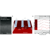
纳米结构金属-金刚石界面上的低密度金刚石状无定形碳

IF 3.1 3区 材料科学 Q2 MATERIALS SCIENCE, MULTIDISCIPLINARY
Brendan McBennett, Yuka Esashi, Nicholas W. Jenkins, Albert Beardo, Yunzhe Shao, Emma E. Nelson, Theodore H. Culman, Begoña Abad, Michael Tanksalvala, Travis D. Frazer, Samuel Marks, Weilun Chao, Sadegh Yazdi, Joshua L. Knobloch, Henry C. Kapteyn, Margaret M. Murnane
{"title":"纳米结构金属-金刚石界面上的低密度金刚石状无定形碳","authors":"Brendan McBennett, Yuka Esashi, Nicholas W. Jenkins, Albert Beardo, Yunzhe Shao, Emma E. Nelson, Theodore H. Culman, Begoña Abad, Michael Tanksalvala, Travis D. Frazer, Samuel Marks, Weilun Chao, Sadegh Yazdi, Joshua L. Knobloch, Henry C. Kapteyn, Margaret M. Murnane","doi":"10.1103/physrevmaterials.8.096001","DOIUrl":null,"url":null,"abstract":"Next-generation nanoelectronic, energy, and quantum technologies require increasingly stringent thermal, optical, mechanical, and electrical properties of component materials, often surpassing the limits of widely used materials such as silicon. Diamond, an ultrawide bandgap semiconductor, is a promising material for these applications because of its very high stiffness, thermal conductivity, and electron mobility. However, incorporating diamond into devices that require high-quality metal-diamond interfaces is challenging. In this work, we use a suite of electron microscopy measurements to reveal an ultrathin amorphous carbon layer that emerges at metal-diamond interfaces after electron beam lithography. Using extreme ultraviolet scatterometry, we nondestructively determine lower bounds on the layer's Young's modulus and thermal conductivity, which at <math xmlns=\"http://www.w3.org/1998/Math/MathML\"><mrow><mo>&gt;</mo><mn>230</mn><mspace width=\"4pt\"></mspace><mi>GPa</mi></mrow></math> and <math xmlns=\"http://www.w3.org/1998/Math/MathML\"><mrow><mo>&gt;</mo><mn>1.1</mn></mrow></math> W/(<math xmlns=\"http://www.w3.org/1998/Math/MathML\"><mrow><mi mathvariant=\"normal\">m</mi><mspace width=\"0.16em\"></mspace><mi mathvariant=\"normal\">K</mi></mrow></math>) are indicative of a diamondlike form of amorphous carbon with high <math xmlns=\"http://www.w3.org/1998/Math/MathML\"><msup><mrow><mi>s</mi><mi>p</mi></mrow><mn>3</mn></msup></math> bonding. However, extreme ultraviolet coherent diffractive imaging reflectometry and energy-dispersive x-ray spectroscopy measurements indicate a low and likely inhomogeneous density in the range of <math xmlns=\"http://www.w3.org/1998/Math/MathML\"><mrow><mn>1</mn><mo>–</mo><mn>2</mn><mspace width=\"4pt\"></mspace><msup><mrow><mi mathvariant=\"normal\">g</mi><mo>/</mo><mi>cm</mi></mrow><mn>3</mn></msup></mrow></math>. The low density of such a stiff and conductive layer could indicate that it contains nanometer-scale voids or atomic-scale vacancies. The appearance of this unusual layer illustrates the nanofabrication challenges for diamond and highlights the need for better techniques to characterize surfaces and interfaces in nanoscale devices.","PeriodicalId":20545,"journal":{"name":"Physical Review Materials","volume":"49 1","pages":""},"PeriodicalIF":3.1000,"publicationDate":"2024-09-16","publicationTypes":"Journal Article","fieldsOfStudy":null,"isOpenAccess":false,"openAccessPdf":"","citationCount":"0","resultStr":"{\"title\":\"Low-density diamondlike amorphous carbon at nanostructured metal-diamond interfaces\",\"authors\":\"Brendan McBennett, Yuka Esashi, Nicholas W. Jenkins, Albert Beardo, Yunzhe Shao, Emma E. Nelson, Theodore H. Culman, Begoña Abad, Michael Tanksalvala, Travis D. Frazer, Samuel Marks, Weilun Chao, Sadegh Yazdi, Joshua L. Knobloch, Henry C. Kapteyn, Margaret M. Murnane\",\"doi\":\"10.1103/physrevmaterials.8.096001\",\"DOIUrl\":null,\"url\":null,\"abstract\":\"Next-generation nanoelectronic, energy, and quantum technologies require increasingly stringent thermal, optical, mechanical, and electrical properties of component materials, often surpassing the limits of widely used materials such as silicon. Diamond, an ultrawide bandgap semiconductor, is a promising material for these applications because of its very high stiffness, thermal conductivity, and electron mobility. However, incorporating diamond into devices that require high-quality metal-diamond interfaces is challenging. In this work, we use a suite of electron microscopy measurements to reveal an ultrathin amorphous carbon layer that emerges at metal-diamond interfaces after electron beam lithography. Using extreme ultraviolet scatterometry, we nondestructively determine lower bounds on the layer's Young's modulus and thermal conductivity, which at <math xmlns=\\\"http://www.w3.org/1998/Math/MathML\\\"><mrow><mo>&gt;</mo><mn>230</mn><mspace width=\\\"4pt\\\"></mspace><mi>GPa</mi></mrow></math> and <math xmlns=\\\"http://www.w3.org/1998/Math/MathML\\\"><mrow><mo>&gt;</mo><mn>1.1</mn></mrow></math> W/(<math xmlns=\\\"http://www.w3.org/1998/Math/MathML\\\"><mrow><mi mathvariant=\\\"normal\\\">m</mi><mspace width=\\\"0.16em\\\"></mspace><mi mathvariant=\\\"normal\\\">K</mi></mrow></math>) are indicative of a diamondlike form of amorphous carbon with high <math xmlns=\\\"http://www.w3.org/1998/Math/MathML\\\"><msup><mrow><mi>s</mi><mi>p</mi></mrow><mn>3</mn></msup></math> bonding. However, extreme ultraviolet coherent diffractive imaging reflectometry and energy-dispersive x-ray spectroscopy measurements indicate a low and likely inhomogeneous density in the range of <math xmlns=\\\"http://www.w3.org/1998/Math/MathML\\\"><mrow><mn>1</mn><mo>–</mo><mn>2</mn><mspace width=\\\"4pt\\\"></mspace><msup><mrow><mi mathvariant=\\\"normal\\\">g</mi><mo>/</mo><mi>cm</mi></mrow><mn>3</mn></msup></mrow></math>. The low density of such a stiff and conductive layer could indicate that it contains nanometer-scale voids or atomic-scale vacancies. The appearance of this unusual layer illustrates the nanofabrication challenges for diamond and highlights the need for better techniques to characterize surfaces and interfaces in nanoscale devices.\",\"PeriodicalId\":20545,\"journal\":{\"name\":\"Physical Review Materials\",\"volume\":\"49 1\",\"pages\":\"\"},\"PeriodicalIF\":3.1000,\"publicationDate\":\"2024-09-16\",\"publicationTypes\":\"Journal Article\",\"fieldsOfStudy\":null,\"isOpenAccess\":false,\"openAccessPdf\":\"\",\"citationCount\":\"0\",\"resultStr\":null,\"platform\":\"Semanticscholar\",\"paperid\":null,\"PeriodicalName\":\"Physical Review Materials\",\"FirstCategoryId\":\"88\",\"ListUrlMain\":\"https://doi.org/10.1103/physrevmaterials.8.096001\",\"RegionNum\":3,\"RegionCategory\":\"材料科学\",\"ArticlePicture\":[],\"TitleCN\":null,\"AbstractTextCN\":null,\"PMCID\":null,\"EPubDate\":\"\",\"PubModel\":\"\",\"JCR\":\"Q2\",\"JCRName\":\"MATERIALS SCIENCE, MULTIDISCIPLINARY\",\"Score\":null,\"Total\":0}","platform":"Semanticscholar","paperid":null,"PeriodicalName":"Physical Review Materials","FirstCategoryId":"88","ListUrlMain":"https://doi.org/10.1103/physrevmaterials.8.096001","RegionNum":3,"RegionCategory":"材料科学","ArticlePicture":[],"TitleCN":null,"AbstractTextCN":null,"PMCID":null,"EPubDate":"","PubModel":"","JCR":"Q2","JCRName":"MATERIALS SCIENCE, MULTIDISCIPLINARY","Score":null,"Total":0}
引用次数: 0

摘要

下一代纳米电子、能源和量子技术对元件材料的热学、光学、机械和电学特性的要求越来越严格,往往超过了硅等广泛使用的材料的极限。金刚石是一种超宽带隙半导体,具有极高的硬度、热导率和电子迁移率,是一种很有前途的应用材料。然而,将金刚石应用到需要高质量金属-金刚石界面的设备中具有挑战性。在这项工作中,我们利用一套电子显微镜测量方法揭示了电子束光刻后在金属-金刚石界面上出现的超薄无定形碳层。利用极紫外散射测量法,我们非破坏性地确定了该层的杨氏模量和热导率的下限,230GPa 和 1.1 W/(mK) 的杨氏模量和热导率表明该层是一种具有高 sp3 键的类似金刚石的无定形碳。然而,极紫外相干衍射成像反射测量法和能量色散 X 射线光谱法的测量结果表明,密度很低,而且很可能不均匀,在 1-2 克/立方厘米的范围内。如此坚硬的导电层密度如此之低,可能表明其中含有纳米级空隙或原子级空位。这种不寻常层的出现说明了金刚石的纳米制造所面临的挑战,并突出表明需要更好的技术来表征纳米级器件的表面和界面。
本文章由计算机程序翻译,如有差异,请以英文原文为准。

Low-density diamondlike amorphous carbon at nanostructured metal-diamond interfaces

Low-density diamondlike amorphous carbon at nanostructured metal-diamond interfaces
Next-generation nanoelectronic, energy, and quantum technologies require increasingly stringent thermal, optical, mechanical, and electrical properties of component materials, often surpassing the limits of widely used materials such as silicon. Diamond, an ultrawide bandgap semiconductor, is a promising material for these applications because of its very high stiffness, thermal conductivity, and electron mobility. However, incorporating diamond into devices that require high-quality metal-diamond interfaces is challenging. In this work, we use a suite of electron microscopy measurements to reveal an ultrathin amorphous carbon layer that emerges at metal-diamond interfaces after electron beam lithography. Using extreme ultraviolet scatterometry, we nondestructively determine lower bounds on the layer's Young's modulus and thermal conductivity, which at >230GPa and >1.1 W/(mK) are indicative of a diamondlike form of amorphous carbon with high sp3 bonding. However, extreme ultraviolet coherent diffractive imaging reflectometry and energy-dispersive x-ray spectroscopy measurements indicate a low and likely inhomogeneous density in the range of 12g/cm3. The low density of such a stiff and conductive layer could indicate that it contains nanometer-scale voids or atomic-scale vacancies. The appearance of this unusual layer illustrates the nanofabrication challenges for diamond and highlights the need for better techniques to characterize surfaces and interfaces in nanoscale devices.
求助全文
通过发布文献求助,成功后即可免费获取论文全文。 去求助
来源期刊
Physical Review Materials
Physical Review Materials Physics and Astronomy-Physics and Astronomy (miscellaneous)
CiteScore
5.80
自引率
5.90%
发文量
611
期刊介绍: Physical Review Materials is a new broad-scope international journal for the multidisciplinary community engaged in research on materials. It is intended to fill a gap in the family of existing Physical Review journals that publish materials research. This field has grown rapidly in recent years and is increasingly being carried out in a way that transcends conventional subject boundaries. The journal was created to provide a common publication and reference source to the expanding community of physicists, materials scientists, chemists, engineers, and researchers in related disciplines that carry out high-quality original research in materials. It will share the same commitment to the high quality expected of all APS publications.
×
引用
GB/T 7714-2015
复制
MLA
复制
APA
复制
导出至
BibTeX EndNote RefMan NoteFirst NoteExpress
×
提示
您的信息不完整,为了账户安全,请先补充。
现在去补充
×
提示
您因"违规操作"
具体请查看互助需知
我知道了
×
提示
确定
请完成安全验证×
copy
已复制链接
快去分享给好友吧!
我知道了
右上角分享
点击右上角分享
0
联系我们:info@booksci.cn Book学术提供免费学术资源搜索服务,方便国内外学者检索中英文文献。致力于提供最便捷和优质的服务体验。 Copyright © 2023 布克学术 All rights reserved.
京ICP备2023020795号-1
ghs 京公网安备 11010802042870号
Book学术文献互助
Book学术文献互助群
群 号:481959085
Book学术官方微信