{"title":"脉冲激光扫描退火法获得的高导电性铜互连薄膜中的晶粒生长和杂质扩散研究","authors":"","doi":"10.1016/j.jmapro.2024.09.039","DOIUrl":null,"url":null,"abstract":"<div><p>The resistivity of the interconnection is a crucial restriction to its performance. In this paper, pulsed laser scanning annealing (PLSA) is proposed as a novel annealing method to reduce the resistance of copper interconnects. The impacts of pulsed laser irradiation on copper interconnect resistance are studied in terms of grain growth and impurity diffusion by experiments and simulations. The temperature gradient generated by laser induces the in-plane and in-depth columnar grain growth, with maximum grain sizes of 17.4 μm and 21.6 μm, respectively. The impurity diffusion is stimulated when the single pulse energy exceeds a threshold at the same laser power density, verified by experiments and calculations. The amount of total escaped impurities and Cl is 83.2 % and 89.2 % higher in PLSA than in thermal annealing, respectively. As a result, copper films with conductivity up to 98.6 % international annealed copper standard were obtained, which makes PLSA a potential application for future advanced interconnects.</p></div>","PeriodicalId":16148,"journal":{"name":"Journal of Manufacturing Processes","volume":null,"pages":null},"PeriodicalIF":6.1000,"publicationDate":"2024-09-15","publicationTypes":"Journal Article","fieldsOfStudy":null,"isOpenAccess":false,"openAccessPdf":"","citationCount":"0","resultStr":"{\"title\":\"Investigation of grain growth and impurity diffusion in highly conductive copper interconnect films obtained by pulsed laser scanning annealing\",\"authors\":\"\",\"doi\":\"10.1016/j.jmapro.2024.09.039\",\"DOIUrl\":null,\"url\":null,\"abstract\":\"<div><p>The resistivity of the interconnection is a crucial restriction to its performance. In this paper, pulsed laser scanning annealing (PLSA) is proposed as a novel annealing method to reduce the resistance of copper interconnects. The impacts of pulsed laser irradiation on copper interconnect resistance are studied in terms of grain growth and impurity diffusion by experiments and simulations. The temperature gradient generated by laser induces the in-plane and in-depth columnar grain growth, with maximum grain sizes of 17.4 μm and 21.6 μm, respectively. The impurity diffusion is stimulated when the single pulse energy exceeds a threshold at the same laser power density, verified by experiments and calculations. The amount of total escaped impurities and Cl is 83.2 % and 89.2 % higher in PLSA than in thermal annealing, respectively. As a result, copper films with conductivity up to 98.6 % international annealed copper standard were obtained, which makes PLSA a potential application for future advanced interconnects.</p></div>\",\"PeriodicalId\":16148,\"journal\":{\"name\":\"Journal of Manufacturing Processes\",\"volume\":null,\"pages\":null},\"PeriodicalIF\":6.1000,\"publicationDate\":\"2024-09-15\",\"publicationTypes\":\"Journal Article\",\"fieldsOfStudy\":null,\"isOpenAccess\":false,\"openAccessPdf\":\"\",\"citationCount\":\"0\",\"resultStr\":null,\"platform\":\"Semanticscholar\",\"paperid\":null,\"PeriodicalName\":\"Journal of Manufacturing Processes\",\"FirstCategoryId\":\"5\",\"ListUrlMain\":\"https://www.sciencedirect.com/science/article/pii/S1526612524009587\",\"RegionNum\":1,\"RegionCategory\":\"工程技术\",\"ArticlePicture\":[],\"TitleCN\":null,\"AbstractTextCN\":null,\"PMCID\":null,\"EPubDate\":\"\",\"PubModel\":\"\",\"JCR\":\"Q1\",\"JCRName\":\"ENGINEERING, MANUFACTURING\",\"Score\":null,\"Total\":0}","platform":"Semanticscholar","paperid":null,"PeriodicalName":"Journal of Manufacturing Processes","FirstCategoryId":"5","ListUrlMain":"https://www.sciencedirect.com/science/article/pii/S1526612524009587","RegionNum":1,"RegionCategory":"工程技术","ArticlePicture":[],"TitleCN":null,"AbstractTextCN":null,"PMCID":null,"EPubDate":"","PubModel":"","JCR":"Q1","JCRName":"ENGINEERING, MANUFACTURING","Score":null,"Total":0}
Investigation of grain growth and impurity diffusion in highly conductive copper interconnect films obtained by pulsed laser scanning annealing
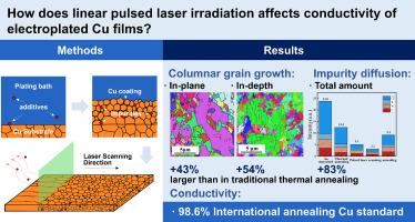
The resistivity of the interconnection is a crucial restriction to its performance. In this paper, pulsed laser scanning annealing (PLSA) is proposed as a novel annealing method to reduce the resistance of copper interconnects. The impacts of pulsed laser irradiation on copper interconnect resistance are studied in terms of grain growth and impurity diffusion by experiments and simulations. The temperature gradient generated by laser induces the in-plane and in-depth columnar grain growth, with maximum grain sizes of 17.4 μm and 21.6 μm, respectively. The impurity diffusion is stimulated when the single pulse energy exceeds a threshold at the same laser power density, verified by experiments and calculations. The amount of total escaped impurities and Cl is 83.2 % and 89.2 % higher in PLSA than in thermal annealing, respectively. As a result, copper films with conductivity up to 98.6 % international annealed copper standard were obtained, which makes PLSA a potential application for future advanced interconnects.
期刊介绍:
The aim of the Journal of Manufacturing Processes (JMP) is to exchange current and future directions of manufacturing processes research, development and implementation, and to publish archival scholarly literature with a view to advancing state-of-the-art manufacturing processes and encouraging innovation for developing new and efficient processes. The journal will also publish from other research communities for rapid communication of innovative new concepts. Special-topic issues on emerging technologies and invited papers will also be published.

 求助内容:
求助内容: 应助结果提醒方式:


