Ingvild Bergsbak, Ørnulf Nordseth, Kjetil K. Saxegaard, Vegard S. Olsen, Holger von Wenckstern, Kristin Bergum
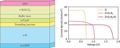
{"title":"25.9% 高效 ZnOxNy/Si 串联太阳能电池的器件模拟","authors":"Ingvild Bergsbak, Ørnulf Nordseth, Kjetil K. Saxegaard, Vegard S. Olsen, Holger von Wenckstern, Kristin Bergum","doi":"10.1002/adts.202400252","DOIUrl":null,"url":null,"abstract":"<p>The novel, high electron mobility material <span></span><math>\n <semantics>\n <mrow>\n <msub>\n <mi>ZnO</mi>\n <mi>x</mi>\n </msub>\n <msub>\n <mi>N</mi>\n <mi>y</mi>\n </msub>\n </mrow>\n <annotation>${\\rm ZnO}_x{\\rm N}_y$</annotation>\n </semantics></math> has been investigated theoretically as an absorber in a two-terminal tandem solar cell. In addition to its high mobility, <span></span><math>\n <semantics>\n <mrow>\n <msub>\n <mi>ZnO</mi>\n <mi>x</mi>\n </msub>\n <msub>\n <mi>N</mi>\n <mi>y</mi>\n </msub>\n </mrow>\n <annotation>${\\rm ZnO}_x{\\rm N}_y$</annotation>\n </semantics></math> can attain sufficiently low carrier concentration to enable <span></span><math>\n <semantics>\n <mrow>\n <mi>p</mi>\n <mi>n</mi>\n </mrow>\n <annotation>$pn$</annotation>\n </semantics></math>-junctions, and has a tunable bandgap around the 1.7 eV range. It is therefore suitable for pairing with a Si-based bottom cell. In addition to the <span></span><math>\n <semantics>\n <mrow>\n <msub>\n <mi>ZnO</mi>\n <mi>x</mi>\n </msub>\n <msub>\n <mi>N</mi>\n <mi>y</mi>\n </msub>\n </mrow>\n <annotation>${\\rm ZnO}_x{\\rm N}_y$</annotation>\n </semantics></math> layer, the tandem cell consists of a <span></span><math>\n <semantics>\n <mrow>\n <msub>\n <mi>Cu</mi>\n <mn>2</mn>\n </msub>\n <mi>O</mi>\n </mrow>\n <annotation>${\\rm Cu}_2{\\rm O}$</annotation>\n </semantics></math> emitter and a Si heterojunction bottom cell. A buffer layer is introduced between the emitter and absorber in the top cell to mediate a large valence band offset that resulted in a poor fill factor, <span></span><math>\n <semantics>\n <mrow>\n <mi>F</mi>\n <mi>F</mi>\n </mrow>\n <annotation>$FF$</annotation>\n </semantics></math>. A <span></span><math>\n <semantics>\n <mrow>\n <msub>\n <mi>ZnO</mi>\n <mi>x</mi>\n </msub>\n <msub>\n <mi>N</mi>\n <mi>y</mi>\n </msub>\n </mrow>\n <annotation>${\\rm ZnO}_x{\\rm N}_y$</annotation>\n </semantics></math> buffer layer bandgap of 1.5 eV gave the highest power conversion efficiency (PCE). The objective is to estimate the optimal performance of <span></span><math>\n <semantics>\n <mrow>\n <msub>\n <mi>ZnO</mi>\n <mi>x</mi>\n </msub>\n <msub>\n <mi>N</mi>\n <mi>y</mi>\n </msub>\n </mrow>\n <annotation>${\\rm ZnO}_x{\\rm N}_y$</annotation>\n </semantics></math> in a tandem solar cell. The dependence of current–voltage (<span></span><math>\n <semantics>\n <mi>J</mi>\n <annotation>$J$</annotation>\n </semantics></math>–<span></span><math>\n <semantics>\n <mi>V</mi>\n <annotation>$V$</annotation>\n </semantics></math>) characteristics on thickness, mobility and carrier concentration in the <span></span><math>\n <semantics>\n <mrow>\n <msub>\n <mi>ZnO</mi>\n <mi>x</mi>\n </msub>\n <msub>\n <mi>N</mi>\n <mi>y</mi>\n </msub>\n </mrow>\n <annotation>${\\rm ZnO}_x{\\rm N}_y$</annotation>\n </semantics></math> layer is evaluated, and found to yield maximum performance with 0.35 <span></span><math>\n <semantics>\n <mrow>\n <mi>μ</mi>\n <mi>m</mi>\n </mrow>\n <annotation>$\\umu {\\rm m}$</annotation>\n </semantics></math>, 250 <span></span><math>\n <semantics>\n <msup>\n <mi>cm</mi>\n <mn>2</mn>\n </msup>\n <annotation>${\\rm cm}^2$</annotation>\n </semantics></math> Vs<sup>–1</sup> and <span></span><math>\n <semantics>\n <msup>\n <mn>10</mn>\n <mn>16</mn>\n </msup>\n <annotation>$10^{16}$</annotation>\n </semantics></math> <span></span><math>\n <semantics>\n <msup>\n <mi>cm</mi>\n <mrow>\n <mo>−</mo>\n <mn>3</mn>\n </mrow>\n </msup>\n <annotation>${\\rm cm}^{-3}$</annotation>\n </semantics></math>, respectively. Using these conditions, the <span></span><math>\n <semantics>\n <mi>J</mi>\n <annotation>$J$</annotation>\n </semantics></math>–<span></span><math>\n <semantics>\n <mi>V</mi>\n <annotation>$V$</annotation>\n </semantics></math> parameters of the device under AM1.5 illumination are short circuit current density, <span></span><math>\n <semantics>\n <mrow>\n <msub>\n <mi>J</mi>\n <mrow>\n <mi>S</mi>\n <mi>C</mi>\n </mrow>\n </msub>\n <mo>=</mo>\n <mn>17.76</mn>\n </mrow>\n <annotation>$J_{SC}=17.76$</annotation>\n </semantics></math> mA <span></span><math>\n <semantics>\n <msup>\n <mi>cm</mi>\n <mrow>\n <mo>−</mo>\n <mn>2</mn>\n </mrow>\n </msup>\n <annotation>${\\mathrm{cm}}^{-2}$</annotation>\n </semantics></math>, open circuit voltage, <span></span><math>\n <semantics>\n <mrow>\n <msub>\n <mi>V</mi>\n <mrow>\n <mi>O</mi>\n <mi>C</mi>\n </mrow>\n </msub>\n <mo>=</mo>\n <mn>1.74</mn>\n </mrow>\n <annotation>$V_{OC}=1.74$</annotation>\n </semantics></math> V, <span></span><math>\n <semantics>\n <mrow>\n <mi>F</mi>\n <mi>F</mi>\n <mo>=</mo>\n <mn>83.8</mn>\n <mo>%</mo>\n </mrow>\n <annotation>$FF=83.8\\%$</annotation>\n </semantics></math> and <span></span><math>\n <semantics>\n <mrow>\n <mi>PCE</mi>\n <mspace></mspace>\n <mo>=</mo>\n <mn>25.9</mn>\n <mo>%</mo>\n </mrow>\n <annotation>${\\rm PCE}\\,=25.9\\%$</annotation>\n </semantics></math>. With this, it is reported on, to the best of the knowledge, the first device simulation based on <span></span><math>\n <semantics>\n <mrow>\n <msub>\n <mi>ZnO</mi>\n <mi>x</mi>\n </msub>\n <msub>\n <mi>N</mi>\n <mi>y</mi>\n </msub>\n </mrow>\n <annotation>${\\rm ZnO}_x{\\rm N}_y$</annotation>\n </semantics></math>.</p>","PeriodicalId":7219,"journal":{"name":"Advanced Theory and Simulations","volume":"7 12","pages":""},"PeriodicalIF":2.9000,"publicationDate":"2024-09-10","publicationTypes":"Journal Article","fieldsOfStudy":null,"isOpenAccess":false,"openAccessPdf":"https://onlinelibrary.wiley.com/doi/epdf/10.1002/adts.202400252","citationCount":"0","resultStr":"{\"title\":\"Device Simulation of 25.9% Efficient \\n \\n \\n \\n ZnO\\n x\\n \\n \\n N\\n y\\n \\n \\n ${\\\\rm ZnO}_x{\\\\rm N}_y$\\n /Si Tandem Solar Cell\",\"authors\":\"Ingvild Bergsbak, Ørnulf Nordseth, Kjetil K. Saxegaard, Vegard S. Olsen, Holger von Wenckstern, Kristin Bergum\",\"doi\":\"10.1002/adts.202400252\",\"DOIUrl\":null,\"url\":null,\"abstract\":\"<p>The novel, high electron mobility material <span></span><math>\\n <semantics>\\n <mrow>\\n <msub>\\n <mi>ZnO</mi>\\n <mi>x</mi>\\n </msub>\\n <msub>\\n <mi>N</mi>\\n <mi>y</mi>\\n </msub>\\n </mrow>\\n <annotation>${\\\\rm ZnO}_x{\\\\rm N}_y$</annotation>\\n </semantics></math> has been investigated theoretically as an absorber in a two-terminal tandem solar cell. In addition to its high mobility, <span></span><math>\\n <semantics>\\n <mrow>\\n <msub>\\n <mi>ZnO</mi>\\n <mi>x</mi>\\n </msub>\\n <msub>\\n <mi>N</mi>\\n <mi>y</mi>\\n </msub>\\n </mrow>\\n <annotation>${\\\\rm ZnO}_x{\\\\rm N}_y$</annotation>\\n </semantics></math> can attain sufficiently low carrier concentration to enable <span></span><math>\\n <semantics>\\n <mrow>\\n <mi>p</mi>\\n <mi>n</mi>\\n </mrow>\\n <annotation>$pn$</annotation>\\n </semantics></math>-junctions, and has a tunable bandgap around the 1.7 eV range. It is therefore suitable for pairing with a Si-based bottom cell. In addition to the <span></span><math>\\n <semantics>\\n <mrow>\\n <msub>\\n <mi>ZnO</mi>\\n <mi>x</mi>\\n </msub>\\n <msub>\\n <mi>N</mi>\\n <mi>y</mi>\\n </msub>\\n </mrow>\\n <annotation>${\\\\rm ZnO}_x{\\\\rm N}_y$</annotation>\\n </semantics></math> layer, the tandem cell consists of a <span></span><math>\\n <semantics>\\n <mrow>\\n <msub>\\n <mi>Cu</mi>\\n <mn>2</mn>\\n </msub>\\n <mi>O</mi>\\n </mrow>\\n <annotation>${\\\\rm Cu}_2{\\\\rm O}$</annotation>\\n </semantics></math> emitter and a Si heterojunction bottom cell. A buffer layer is introduced between the emitter and absorber in the top cell to mediate a large valence band offset that resulted in a poor fill factor, <span></span><math>\\n <semantics>\\n <mrow>\\n <mi>F</mi>\\n <mi>F</mi>\\n </mrow>\\n <annotation>$FF$</annotation>\\n </semantics></math>. A <span></span><math>\\n <semantics>\\n <mrow>\\n <msub>\\n <mi>ZnO</mi>\\n <mi>x</mi>\\n </msub>\\n <msub>\\n <mi>N</mi>\\n <mi>y</mi>\\n </msub>\\n </mrow>\\n <annotation>${\\\\rm ZnO}_x{\\\\rm N}_y$</annotation>\\n </semantics></math> buffer layer bandgap of 1.5 eV gave the highest power conversion efficiency (PCE). The objective is to estimate the optimal performance of <span></span><math>\\n <semantics>\\n <mrow>\\n <msub>\\n <mi>ZnO</mi>\\n <mi>x</mi>\\n </msub>\\n <msub>\\n <mi>N</mi>\\n <mi>y</mi>\\n </msub>\\n </mrow>\\n <annotation>${\\\\rm ZnO}_x{\\\\rm N}_y$</annotation>\\n </semantics></math> in a tandem solar cell. The dependence of current–voltage (<span></span><math>\\n <semantics>\\n <mi>J</mi>\\n <annotation>$J$</annotation>\\n </semantics></math>–<span></span><math>\\n <semantics>\\n <mi>V</mi>\\n <annotation>$V$</annotation>\\n </semantics></math>) characteristics on thickness, mobility and carrier concentration in the <span></span><math>\\n <semantics>\\n <mrow>\\n <msub>\\n <mi>ZnO</mi>\\n <mi>x</mi>\\n </msub>\\n <msub>\\n <mi>N</mi>\\n <mi>y</mi>\\n </msub>\\n </mrow>\\n <annotation>${\\\\rm ZnO}_x{\\\\rm N}_y$</annotation>\\n </semantics></math> layer is evaluated, and found to yield maximum performance with 0.35 <span></span><math>\\n <semantics>\\n <mrow>\\n <mi>μ</mi>\\n <mi>m</mi>\\n </mrow>\\n <annotation>$\\\\umu {\\\\rm m}$</annotation>\\n </semantics></math>, 250 <span></span><math>\\n <semantics>\\n <msup>\\n <mi>cm</mi>\\n <mn>2</mn>\\n </msup>\\n <annotation>${\\\\rm cm}^2$</annotation>\\n </semantics></math> Vs<sup>–1</sup> and <span></span><math>\\n <semantics>\\n <msup>\\n <mn>10</mn>\\n <mn>16</mn>\\n </msup>\\n <annotation>$10^{16}$</annotation>\\n </semantics></math> <span></span><math>\\n <semantics>\\n <msup>\\n <mi>cm</mi>\\n <mrow>\\n <mo>−</mo>\\n <mn>3</mn>\\n </mrow>\\n </msup>\\n <annotation>${\\\\rm cm}^{-3}$</annotation>\\n </semantics></math>, respectively. Using these conditions, the <span></span><math>\\n <semantics>\\n <mi>J</mi>\\n <annotation>$J$</annotation>\\n </semantics></math>–<span></span><math>\\n <semantics>\\n <mi>V</mi>\\n <annotation>$V$</annotation>\\n </semantics></math> parameters of the device under AM1.5 illumination are short circuit current density, <span></span><math>\\n <semantics>\\n <mrow>\\n <msub>\\n <mi>J</mi>\\n <mrow>\\n <mi>S</mi>\\n <mi>C</mi>\\n </mrow>\\n </msub>\\n <mo>=</mo>\\n <mn>17.76</mn>\\n </mrow>\\n <annotation>$J_{SC}=17.76$</annotation>\\n </semantics></math> mA <span></span><math>\\n <semantics>\\n <msup>\\n <mi>cm</mi>\\n <mrow>\\n <mo>−</mo>\\n <mn>2</mn>\\n </mrow>\\n </msup>\\n <annotation>${\\\\mathrm{cm}}^{-2}$</annotation>\\n </semantics></math>, open circuit voltage, <span></span><math>\\n <semantics>\\n <mrow>\\n <msub>\\n <mi>V</mi>\\n <mrow>\\n <mi>O</mi>\\n <mi>C</mi>\\n </mrow>\\n </msub>\\n <mo>=</mo>\\n <mn>1.74</mn>\\n </mrow>\\n <annotation>$V_{OC}=1.74$</annotation>\\n </semantics></math> V, <span></span><math>\\n <semantics>\\n <mrow>\\n <mi>F</mi>\\n <mi>F</mi>\\n <mo>=</mo>\\n <mn>83.8</mn>\\n <mo>%</mo>\\n </mrow>\\n <annotation>$FF=83.8\\\\%$</annotation>\\n </semantics></math> and <span></span><math>\\n <semantics>\\n <mrow>\\n <mi>PCE</mi>\\n <mspace></mspace>\\n <mo>=</mo>\\n <mn>25.9</mn>\\n <mo>%</mo>\\n </mrow>\\n <annotation>${\\\\rm PCE}\\\\,=25.9\\\\%$</annotation>\\n </semantics></math>. With this, it is reported on, to the best of the knowledge, the first device simulation based on <span></span><math>\\n <semantics>\\n <mrow>\\n <msub>\\n <mi>ZnO</mi>\\n <mi>x</mi>\\n </msub>\\n <msub>\\n <mi>N</mi>\\n <mi>y</mi>\\n </msub>\\n </mrow>\\n <annotation>${\\\\rm ZnO}_x{\\\\rm N}_y$</annotation>\\n </semantics></math>.</p>\",\"PeriodicalId\":7219,\"journal\":{\"name\":\"Advanced Theory and Simulations\",\"volume\":\"7 12\",\"pages\":\"\"},\"PeriodicalIF\":2.9000,\"publicationDate\":\"2024-09-10\",\"publicationTypes\":\"Journal Article\",\"fieldsOfStudy\":null,\"isOpenAccess\":false,\"openAccessPdf\":\"https://onlinelibrary.wiley.com/doi/epdf/10.1002/adts.202400252\",\"citationCount\":\"0\",\"resultStr\":null,\"platform\":\"Semanticscholar\",\"paperid\":null,\"PeriodicalName\":\"Advanced Theory and Simulations\",\"FirstCategoryId\":\"5\",\"ListUrlMain\":\"https://onlinelibrary.wiley.com/doi/10.1002/adts.202400252\",\"RegionNum\":4,\"RegionCategory\":\"工程技术\",\"ArticlePicture\":[],\"TitleCN\":null,\"AbstractTextCN\":null,\"PMCID\":null,\"EPubDate\":\"\",\"PubModel\":\"\",\"JCR\":\"Q1\",\"JCRName\":\"MULTIDISCIPLINARY SCIENCES\",\"Score\":null,\"Total\":0}","platform":"Semanticscholar","paperid":null,"PeriodicalName":"Advanced Theory and Simulations","FirstCategoryId":"5","ListUrlMain":"https://onlinelibrary.wiley.com/doi/10.1002/adts.202400252","RegionNum":4,"RegionCategory":"工程技术","ArticlePicture":[],"TitleCN":null,"AbstractTextCN":null,"PMCID":null,"EPubDate":"","PubModel":"","JCR":"Q1","JCRName":"MULTIDISCIPLINARY SCIENCES","Score":null,"Total":0}
Device Simulation of 25.9% Efficient
ZnO
x
N
y
${\rm ZnO}_x{\rm N}_y$
/Si Tandem Solar Cell
The novel, high electron mobility material has been investigated theoretically as an absorber in a two-terminal tandem solar cell. In addition to its high mobility, can attain sufficiently low carrier concentration to enable -junctions, and has a tunable bandgap around the 1.7 eV range. It is therefore suitable for pairing with a Si-based bottom cell. In addition to the layer, the tandem cell consists of a emitter and a Si heterojunction bottom cell. A buffer layer is introduced between the emitter and absorber in the top cell to mediate a large valence band offset that resulted in a poor fill factor, . A buffer layer bandgap of 1.5 eV gave the highest power conversion efficiency (PCE). The objective is to estimate the optimal performance of in a tandem solar cell. The dependence of current–voltage (–) characteristics on thickness, mobility and carrier concentration in the layer is evaluated, and found to yield maximum performance with 0.35 , 250 Vs–1 and , respectively. Using these conditions, the – parameters of the device under AM1.5 illumination are short circuit current density, mA , open circuit voltage, V, and . With this, it is reported on, to the best of the knowledge, the first device simulation based on .
期刊介绍:
Advanced Theory and Simulations is an interdisciplinary, international, English-language journal that publishes high-quality scientific results focusing on the development and application of theoretical methods, modeling and simulation approaches in all natural science and medicine areas, including:
materials, chemistry, condensed matter physics
engineering, energy
life science, biology, medicine
atmospheric/environmental science, climate science
planetary science, astronomy, cosmology
method development, numerical methods, statistics

 求助内容:
求助内容: 应助结果提醒方式:


