{"title":"面内铁电使单层 MoS2 晶体管中的滞后减少","authors":"Mingxuan Yuan, Binbin Zhang, Jiliang Cai, Jiaqi Zhang, Yue Lu, Shuo Qiao, Kecheng Cao, Hao Deng, Qingqing Ji","doi":"10.1002/cnl2.148","DOIUrl":null,"url":null,"abstract":"<p>Two-dimensional (2D) semiconductors, such as monolayer MoS<sub>2</sub>, has emerged as a profound material platform in the post-Moore era due to their versatile applications for high-performance transistors, memories, photodetectors, neuristors, and so on. Nevertheless, the inherent defects in these atomically thin materials have given rise to significant hysteresis in their field-effect transistors (FETs), resulting in shifted threshold voltages and elevated power consumptions not only on single-device levels but also at circuitry scales. We herein report that, by vertically integrating an in-plane ferroelectric, NbOCl<sub>2</sub>, with monolayer MoS<sub>2</sub> FETs, the hysteresis in both the output and transfer curves of the latter can be greatly suppressed, which we attribute to compensated electromigration currents by the polarization currents of the 2D ferroelectric. This work opens a new avenue to hysteresis-free 2D transistors without necessitating defect-free channels, thus allowing for their use in high driving-voltage scenarios such as power electronics.</p>","PeriodicalId":100214,"journal":{"name":"Carbon Neutralization","volume":"3 4","pages":"700-709"},"PeriodicalIF":0.0000,"publicationDate":"2024-06-17","publicationTypes":"Journal Article","fieldsOfStudy":null,"isOpenAccess":false,"openAccessPdf":"https://onlinelibrary.wiley.com/doi/epdf/10.1002/cnl2.148","citationCount":"0","resultStr":"{\"title\":\"In-plane ferroelectrics enabling reduced hysteresis in monolayer MoS2 transistors\",\"authors\":\"Mingxuan Yuan, Binbin Zhang, Jiliang Cai, Jiaqi Zhang, Yue Lu, Shuo Qiao, Kecheng Cao, Hao Deng, Qingqing Ji\",\"doi\":\"10.1002/cnl2.148\",\"DOIUrl\":null,\"url\":null,\"abstract\":\"<p>Two-dimensional (2D) semiconductors, such as monolayer MoS<sub>2</sub>, has emerged as a profound material platform in the post-Moore era due to their versatile applications for high-performance transistors, memories, photodetectors, neuristors, and so on. Nevertheless, the inherent defects in these atomically thin materials have given rise to significant hysteresis in their field-effect transistors (FETs), resulting in shifted threshold voltages and elevated power consumptions not only on single-device levels but also at circuitry scales. We herein report that, by vertically integrating an in-plane ferroelectric, NbOCl<sub>2</sub>, with monolayer MoS<sub>2</sub> FETs, the hysteresis in both the output and transfer curves of the latter can be greatly suppressed, which we attribute to compensated electromigration currents by the polarization currents of the 2D ferroelectric. This work opens a new avenue to hysteresis-free 2D transistors without necessitating defect-free channels, thus allowing for their use in high driving-voltage scenarios such as power electronics.</p>\",\"PeriodicalId\":100214,\"journal\":{\"name\":\"Carbon Neutralization\",\"volume\":\"3 4\",\"pages\":\"700-709\"},\"PeriodicalIF\":0.0000,\"publicationDate\":\"2024-06-17\",\"publicationTypes\":\"Journal Article\",\"fieldsOfStudy\":null,\"isOpenAccess\":false,\"openAccessPdf\":\"https://onlinelibrary.wiley.com/doi/epdf/10.1002/cnl2.148\",\"citationCount\":\"0\",\"resultStr\":null,\"platform\":\"Semanticscholar\",\"paperid\":null,\"PeriodicalName\":\"Carbon Neutralization\",\"FirstCategoryId\":\"1085\",\"ListUrlMain\":\"https://onlinelibrary.wiley.com/doi/10.1002/cnl2.148\",\"RegionNum\":0,\"RegionCategory\":null,\"ArticlePicture\":[],\"TitleCN\":null,\"AbstractTextCN\":null,\"PMCID\":null,\"EPubDate\":\"\",\"PubModel\":\"\",\"JCR\":\"\",\"JCRName\":\"\",\"Score\":null,\"Total\":0}","platform":"Semanticscholar","paperid":null,"PeriodicalName":"Carbon Neutralization","FirstCategoryId":"1085","ListUrlMain":"https://onlinelibrary.wiley.com/doi/10.1002/cnl2.148","RegionNum":0,"RegionCategory":null,"ArticlePicture":[],"TitleCN":null,"AbstractTextCN":null,"PMCID":null,"EPubDate":"","PubModel":"","JCR":"","JCRName":"","Score":null,"Total":0}
引用次数: 0
摘要
二维(2D)半导体,如单层 MoS2,因其在高性能晶体管、存储器、光电探测器、神经管等方面的广泛应用,已成为后摩尔时代的一个重要材料平台。然而,这些原子级薄材料的固有缺陷导致其场效应晶体管(FET)出现明显的滞后现象,不仅在单个器件层面,而且在电路层面都会造成阈值电压偏移和功耗升高。我们在此报告,通过将平面内铁电 NbOCl2 与单层 MoS2 FET 垂直集成,后者的输出和传输曲线中的滞后现象可以得到极大的抑制,我们将其归因于二维铁电的极化电流补偿了电迁移电流。这项研究为实现无滞后二维晶体管开辟了一条新的途径,无需无缺陷沟道,因此可用于电力电子器件等高驱动电压场合。
In-plane ferroelectrics enabling reduced hysteresis in monolayer MoS2 transistors
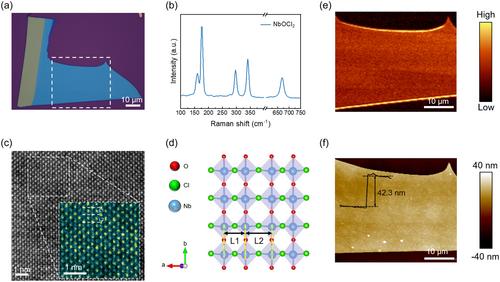
Two-dimensional (2D) semiconductors, such as monolayer MoS2, has emerged as a profound material platform in the post-Moore era due to their versatile applications for high-performance transistors, memories, photodetectors, neuristors, and so on. Nevertheless, the inherent defects in these atomically thin materials have given rise to significant hysteresis in their field-effect transistors (FETs), resulting in shifted threshold voltages and elevated power consumptions not only on single-device levels but also at circuitry scales. We herein report that, by vertically integrating an in-plane ferroelectric, NbOCl2, with monolayer MoS2 FETs, the hysteresis in both the output and transfer curves of the latter can be greatly suppressed, which we attribute to compensated electromigration currents by the polarization currents of the 2D ferroelectric. This work opens a new avenue to hysteresis-free 2D transistors without necessitating defect-free channels, thus allowing for their use in high driving-voltage scenarios such as power electronics.

 求助内容:
求助内容: 应助结果提醒方式:


