在石墨烯/超导体双层中观测到第二个狄拉克点

IF 3.1 3区 材料科学 Q2 MATERIALS SCIENCE, MULTIDISCIPLINARY
Gopi Nath Daptary, Eyal Walach, Udit Khanna, Efrat Shimshoni, Aviad Frydman
{"title":"在石墨烯/超导体双层中观测到第二个狄拉克点","authors":"Gopi Nath Daptary, Eyal Walach, Udit Khanna, Efrat Shimshoni, Aviad Frydman","doi":"10.1103/physrevmaterials.8.084802","DOIUrl":null,"url":null,"abstract":"Two-dimensional (2D) materials have attracted vast research interest since the breakthrough discovery of graphene. One major benefit of such systems is the ability to tune the Fermi level through the charge neutrality point between electron and hole doping. Here we show that single layer graphene coupled to the low-density superconductor indium oxide (InO) exhibits two charge neutrality points, each of them representing electronic regions in which the carrier density can be tuned from hole to electron dominated. This is not seen in clean graphene or in a bilayer where the carrier density is extremely low. We suggest that the second charge neutrality point results from regions in the graphene layer just below superconducting islands in InO, where pairing is induced via the proximity effect; gating of this hybrid system therefore allows the tuning from hole to electron superconductivity through an ultralow carrier density regime. We propose this as a “superconducting Dirac point (SDP)” where intravalley scattering is greatly enhanced. Our results suggest that the electronic states around SDP behave like those in a strongly coupled superconductor.","PeriodicalId":20545,"journal":{"name":"Physical Review Materials","volume":"51 1","pages":""},"PeriodicalIF":3.1000,"publicationDate":"2024-08-01","publicationTypes":"Journal Article","fieldsOfStudy":null,"isOpenAccess":false,"openAccessPdf":"","citationCount":"0","resultStr":"{\"title\":\"Observation of a second Dirac point in a graphene/superconductor bilayer\",\"authors\":\"Gopi Nath Daptary, Eyal Walach, Udit Khanna, Efrat Shimshoni, Aviad Frydman\",\"doi\":\"10.1103/physrevmaterials.8.084802\",\"DOIUrl\":null,\"url\":null,\"abstract\":\"Two-dimensional (2D) materials have attracted vast research interest since the breakthrough discovery of graphene. One major benefit of such systems is the ability to tune the Fermi level through the charge neutrality point between electron and hole doping. Here we show that single layer graphene coupled to the low-density superconductor indium oxide (InO) exhibits two charge neutrality points, each of them representing electronic regions in which the carrier density can be tuned from hole to electron dominated. This is not seen in clean graphene or in a bilayer where the carrier density is extremely low. We suggest that the second charge neutrality point results from regions in the graphene layer just below superconducting islands in InO, where pairing is induced via the proximity effect; gating of this hybrid system therefore allows the tuning from hole to electron superconductivity through an ultralow carrier density regime. We propose this as a “superconducting Dirac point (SDP)” where intravalley scattering is greatly enhanced. Our results suggest that the electronic states around SDP behave like those in a strongly coupled superconductor.\",\"PeriodicalId\":20545,\"journal\":{\"name\":\"Physical Review Materials\",\"volume\":\"51 1\",\"pages\":\"\"},\"PeriodicalIF\":3.1000,\"publicationDate\":\"2024-08-01\",\"publicationTypes\":\"Journal Article\",\"fieldsOfStudy\":null,\"isOpenAccess\":false,\"openAccessPdf\":\"\",\"citationCount\":\"0\",\"resultStr\":null,\"platform\":\"Semanticscholar\",\"paperid\":null,\"PeriodicalName\":\"Physical Review Materials\",\"FirstCategoryId\":\"88\",\"ListUrlMain\":\"https://doi.org/10.1103/physrevmaterials.8.084802\",\"RegionNum\":3,\"RegionCategory\":\"材料科学\",\"ArticlePicture\":[],\"TitleCN\":null,\"AbstractTextCN\":null,\"PMCID\":null,\"EPubDate\":\"\",\"PubModel\":\"\",\"JCR\":\"Q2\",\"JCRName\":\"MATERIALS SCIENCE, MULTIDISCIPLINARY\",\"Score\":null,\"Total\":0}","platform":"Semanticscholar","paperid":null,"PeriodicalName":"Physical Review Materials","FirstCategoryId":"88","ListUrlMain":"https://doi.org/10.1103/physrevmaterials.8.084802","RegionNum":3,"RegionCategory":"材料科学","ArticlePicture":[],"TitleCN":null,"AbstractTextCN":null,"PMCID":null,"EPubDate":"","PubModel":"","JCR":"Q2","JCRName":"MATERIALS SCIENCE, MULTIDISCIPLINARY","Score":null,"Total":0}
引用次数: 0

摘要

自石墨烯的突破性发现以来,二维(2D)材料引起了广泛的研究兴趣。这类系统的一个主要优点是能够通过电子和空穴掺杂之间的电荷中性点来调节费米级。在这里,我们展示了与低密度超导体氧化铟(InO)耦合的单层石墨烯呈现出两个电荷中性点,每个电荷中性点都代表着电子区域,在这些电子区域中,载流子密度可以从空穴主导调整为电子主导。这在干净的石墨烯或载流子密度极低的双电层中是看不到的。我们认为,第二个电荷中性点来自石墨烯层中 InO 超导岛下方的区域,在这些区域中,配对是通过邻近效应诱导的;因此,这种混合系统的门控可以通过超低载流子密度机制实现从空穴到电子的超导调节。我们提出这是一个 "超导狄拉克点(SDP)",在这里,谷内散射大大增强。我们的研究结果表明,SDP 附近的电子态表现与强耦合超导体中的电子态类似。
本文章由计算机程序翻译,如有差异,请以英文原文为准。

Observation of a second Dirac point in a graphene/superconductor bilayer

Observation of a second Dirac point in a graphene/superconductor bilayer
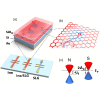
Two-dimensional (2D) materials have attracted vast research interest since the breakthrough discovery of graphene. One major benefit of such systems is the ability to tune the Fermi level through the charge neutrality point between electron and hole doping. Here we show that single layer graphene coupled to the low-density superconductor indium oxide (InO) exhibits two charge neutrality points, each of them representing electronic regions in which the carrier density can be tuned from hole to electron dominated. This is not seen in clean graphene or in a bilayer where the carrier density is extremely low. We suggest that the second charge neutrality point results from regions in the graphene layer just below superconducting islands in InO, where pairing is induced via the proximity effect; gating of this hybrid system therefore allows the tuning from hole to electron superconductivity through an ultralow carrier density regime. We propose this as a “superconducting Dirac point (SDP)” where intravalley scattering is greatly enhanced. Our results suggest that the electronic states around SDP behave like those in a strongly coupled superconductor.
求助全文
通过发布文献求助,成功后即可免费获取论文全文。 去求助
来源期刊
Physical Review Materials
Physical Review Materials Physics and Astronomy-Physics and Astronomy (miscellaneous)
CiteScore
5.80
自引率
5.90%
发文量
611
期刊介绍: Physical Review Materials is a new broad-scope international journal for the multidisciplinary community engaged in research on materials. It is intended to fill a gap in the family of existing Physical Review journals that publish materials research. This field has grown rapidly in recent years and is increasingly being carried out in a way that transcends conventional subject boundaries. The journal was created to provide a common publication and reference source to the expanding community of physicists, materials scientists, chemists, engineers, and researchers in related disciplines that carry out high-quality original research in materials. It will share the same commitment to the high quality expected of all APS publications.
×
引用
GB/T 7714-2015
复制
MLA
复制
APA
复制
导出至
BibTeX EndNote RefMan NoteFirst NoteExpress
×
提示
您的信息不完整,为了账户安全,请先补充。
现在去补充
×
提示
您因"违规操作"
具体请查看互助需知
我知道了
×
提示
确定
请完成安全验证×
copy
已复制链接
快去分享给好友吧!
我知道了
右上角分享
点击右上角分享
0
联系我们:info@booksci.cn Book学术提供免费学术资源搜索服务,方便国内外学者检索中英文文献。致力于提供最便捷和优质的服务体验。 Copyright © 2023 布克学术 All rights reserved.
京ICP备2023020795号-1
ghs 京公网安备 11010802042870号
Book学术文献互助
Book学术文献互助群
群 号:481959085
Book学术官方微信