{"title":"操纵 MoS2 光生载流子行为的亚纳米簇装饰","authors":"Ran Duan, Weihong Qi, Kewei Tang, Weimin Liu","doi":"10.1002/inf2.12610","DOIUrl":null,"url":null,"abstract":"<p>For most applications based on the photoelectric effect, uncontrollable photogenerated carrier behavior, such as trapping and recombination, is a common issue that reduces the carrier utilization efficiency. Herein, a sub-nano cluster (Pd, Ru, and PdRu alloy) decoration strategy is proposed to manipulate the photogenerated carrier behavior in MoS<sub>2</sub> to optimize the optoelectronic properties. After decoration, electrons can flow into sub-nano cluster through Pd<span></span>S bonds and then return to MoS<sub>2</sub> through Ru<span></span>S bonds at the sub-nano cluster/MoS<sub>2</sub> interface when holes are left in the channel for collection to achieve efficient carrier separation. In addition, the formation of metal<span></span>S bonds also leads to the generation of mid-gap states, which enables light absorption over a wide wavelength range. Therefore, the photodetector based on PdRu/MoS<sub>2</sub> shows broadband photodetection ability from 532 to 1550 nm with high responsivity/external quantum efficiency of 310.8 A W<sup>−1</sup>/7 × 10<sup>4</sup>% (532 nm), 4.2 A W<sup>−1</sup>/527% (980 nm), and 7.14 mA W<sup>−1</sup>/0.5% (1550 nm), as well as a fast response speed (rise/decay time of 11.5/12.0 ms). Our work offers new insight into manipulating the photogenerated carrier behavior to optimize the performance of semiconducting 2D materials for practical optoelectronic applications.</p><p>\n <figure>\n <div><picture>\n <source></source></picture><p></p>\n </div>\n </figure></p>","PeriodicalId":48538,"journal":{"name":"Infomat","volume":"7 2","pages":""},"PeriodicalIF":22.7000,"publicationDate":"2024-07-21","publicationTypes":"Journal Article","fieldsOfStudy":null,"isOpenAccess":false,"openAccessPdf":"https://onlinelibrary.wiley.com/doi/epdf/10.1002/inf2.12610","citationCount":"0","resultStr":"{\"title\":\"Sub-nano cluster decoration for the manipulation of the photogenerated carrier behavior of MoS2\",\"authors\":\"Ran Duan, Weihong Qi, Kewei Tang, Weimin Liu\",\"doi\":\"10.1002/inf2.12610\",\"DOIUrl\":null,\"url\":null,\"abstract\":\"<p>For most applications based on the photoelectric effect, uncontrollable photogenerated carrier behavior, such as trapping and recombination, is a common issue that reduces the carrier utilization efficiency. Herein, a sub-nano cluster (Pd, Ru, and PdRu alloy) decoration strategy is proposed to manipulate the photogenerated carrier behavior in MoS<sub>2</sub> to optimize the optoelectronic properties. After decoration, electrons can flow into sub-nano cluster through Pd<span></span>S bonds and then return to MoS<sub>2</sub> through Ru<span></span>S bonds at the sub-nano cluster/MoS<sub>2</sub> interface when holes are left in the channel for collection to achieve efficient carrier separation. In addition, the formation of metal<span></span>S bonds also leads to the generation of mid-gap states, which enables light absorption over a wide wavelength range. Therefore, the photodetector based on PdRu/MoS<sub>2</sub> shows broadband photodetection ability from 532 to 1550 nm with high responsivity/external quantum efficiency of 310.8 A W<sup>−1</sup>/7 × 10<sup>4</sup>% (532 nm), 4.2 A W<sup>−1</sup>/527% (980 nm), and 7.14 mA W<sup>−1</sup>/0.5% (1550 nm), as well as a fast response speed (rise/decay time of 11.5/12.0 ms). Our work offers new insight into manipulating the photogenerated carrier behavior to optimize the performance of semiconducting 2D materials for practical optoelectronic applications.</p><p>\\n <figure>\\n <div><picture>\\n <source></source></picture><p></p>\\n </div>\\n </figure></p>\",\"PeriodicalId\":48538,\"journal\":{\"name\":\"Infomat\",\"volume\":\"7 2\",\"pages\":\"\"},\"PeriodicalIF\":22.7000,\"publicationDate\":\"2024-07-21\",\"publicationTypes\":\"Journal Article\",\"fieldsOfStudy\":null,\"isOpenAccess\":false,\"openAccessPdf\":\"https://onlinelibrary.wiley.com/doi/epdf/10.1002/inf2.12610\",\"citationCount\":\"0\",\"resultStr\":null,\"platform\":\"Semanticscholar\",\"paperid\":null,\"PeriodicalName\":\"Infomat\",\"FirstCategoryId\":\"88\",\"ListUrlMain\":\"https://onlinelibrary.wiley.com/doi/10.1002/inf2.12610\",\"RegionNum\":1,\"RegionCategory\":\"材料科学\",\"ArticlePicture\":[],\"TitleCN\":null,\"AbstractTextCN\":null,\"PMCID\":null,\"EPubDate\":\"\",\"PubModel\":\"\",\"JCR\":\"Q1\",\"JCRName\":\"MATERIALS SCIENCE, MULTIDISCIPLINARY\",\"Score\":null,\"Total\":0}","platform":"Semanticscholar","paperid":null,"PeriodicalName":"Infomat","FirstCategoryId":"88","ListUrlMain":"https://onlinelibrary.wiley.com/doi/10.1002/inf2.12610","RegionNum":1,"RegionCategory":"材料科学","ArticlePicture":[],"TitleCN":null,"AbstractTextCN":null,"PMCID":null,"EPubDate":"","PubModel":"","JCR":"Q1","JCRName":"MATERIALS SCIENCE, MULTIDISCIPLINARY","Score":null,"Total":0}
Sub-nano cluster decoration for the manipulation of the photogenerated carrier behavior of MoS2
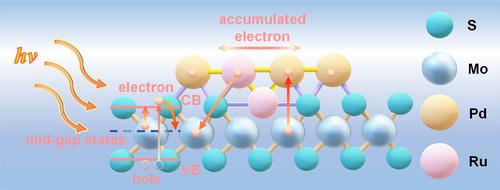
For most applications based on the photoelectric effect, uncontrollable photogenerated carrier behavior, such as trapping and recombination, is a common issue that reduces the carrier utilization efficiency. Herein, a sub-nano cluster (Pd, Ru, and PdRu alloy) decoration strategy is proposed to manipulate the photogenerated carrier behavior in MoS2 to optimize the optoelectronic properties. After decoration, electrons can flow into sub-nano cluster through PdS bonds and then return to MoS2 through RuS bonds at the sub-nano cluster/MoS2 interface when holes are left in the channel for collection to achieve efficient carrier separation. In addition, the formation of metalS bonds also leads to the generation of mid-gap states, which enables light absorption over a wide wavelength range. Therefore, the photodetector based on PdRu/MoS2 shows broadband photodetection ability from 532 to 1550 nm with high responsivity/external quantum efficiency of 310.8 A W−1/7 × 104% (532 nm), 4.2 A W−1/527% (980 nm), and 7.14 mA W−1/0.5% (1550 nm), as well as a fast response speed (rise/decay time of 11.5/12.0 ms). Our work offers new insight into manipulating the photogenerated carrier behavior to optimize the performance of semiconducting 2D materials for practical optoelectronic applications.
期刊介绍:
InfoMat, an interdisciplinary and open-access journal, caters to the growing scientific interest in novel materials with unique electrical, optical, and magnetic properties, focusing on their applications in the rapid advancement of information technology. The journal serves as a high-quality platform for researchers across diverse scientific areas to share their findings, critical opinions, and foster collaboration between the materials science and information technology communities.

 求助内容:
求助内容: 应助结果提醒方式:


