Yuan Xu, Minhong Jiang, Xinkang Liu, Yujiao Zeng, Shixuan Cao, Yujiao Ouyang, Jianwei Song and Guanghui Rao
{"title":"无种子固态晶体生长法生长的铜、铋和锰共掺杂 K0.5Na0.5NbO3 单晶的结构和电学特性","authors":"Yuan Xu, Minhong Jiang, Xinkang Liu, Yujiao Zeng, Shixuan Cao, Yujiao Ouyang, Jianwei Song and Guanghui Rao","doi":"10.1039/D4CE00502C","DOIUrl":null,"url":null,"abstract":"<p >K<small><sub>0.5</sub></small>Na<small><sub>0.5</sub></small>NbO<small><sub>3</sub></small> (KNN) crystals have great application prospects due to their excellent piezoelectric properties, high Curie temperature, and environmental friendliness. Currently, KNN crystals grown by the seed-free solid-state crystal growth (SFSSCG) method exhibit relatively high dielectric loss. In order to reduce their dielectric loss, Cu, Bi and Mn co-doped KNN lead-free piezoelectric single crystals were prepared by the SFSSCG method. The effects of the CuO doping content on the structure and electrical properties of (1 − <em>x</em>)(0.996KNN–0.004BiMnO<small><sub>3</sub></small>)–<em>x</em>CuO crystals were systematically studied. The results show that an appropriate doping amount of CuO is beneficial for the growth of the crystals and the improvement of electrical properties. When the diameter of the billets is 40 mm, the maximum crystal size of 25 × 21 × 2 mm<small><sup>3</sup></small> is obtained. All crystals have a typical perovskite structure almost with a single orthorhombic phase and are very compact almost without holes. The minimum average domain width of 276 nm is obtained for the crystal at <em>x</em> = 0.005. The KNN crystals exhibit normal ferroelectric characteristics and a space-charge-limited-conduction (SCLC) mechanism. The introduction of Cu<small><sup>2+</sup></small> ions reduces the dielectric loss of the crystal and increases its piezoelectric and dielectric properties. The Cu, Bi and Mn co-doped KNN crystals achieve excellent comprehensive properties: <em>d</em><small><sub>33</sub></small> = 314 pC N<small><sup>−1</sup></small>, <em>P</em><small><sub>r</sub></small> = 29.9 μC cm<small><sup>−2</sup></small>, <em>E</em><small><sub>c</sub></small> = 10.1 kV cm<small><sup>−1</sup></small>, <img> = 869 pm V<small><sup>−1</sup></small>, <em>Q</em><small><sub>m</sub></small> = 56.8, <em>K</em><small><sub>t</sub></small> = 0.38, tan <em>δ</em> = 0.013 and <em>T</em><small><sub>C</sub></small> = 409 °C. This provides a route to improve the electrical properties of KNN-based crystals.</p>","PeriodicalId":70,"journal":{"name":"CrystEngComm","volume":" 31","pages":" 4146-4155"},"PeriodicalIF":2.6000,"publicationDate":"2024-07-12","publicationTypes":"Journal Article","fieldsOfStudy":null,"isOpenAccess":false,"openAccessPdf":"","citationCount":"0","resultStr":"{\"title\":\"Structure and electrical properties of Cu, Bi and Mn co-doped K0.5Na0.5NbO3 single crystals grown by the seed-free solid state crystal growth method\",\"authors\":\"Yuan Xu, Minhong Jiang, Xinkang Liu, Yujiao Zeng, Shixuan Cao, Yujiao Ouyang, Jianwei Song and Guanghui Rao\",\"doi\":\"10.1039/D4CE00502C\",\"DOIUrl\":null,\"url\":null,\"abstract\":\"<p >K<small><sub>0.5</sub></small>Na<small><sub>0.5</sub></small>NbO<small><sub>3</sub></small> (KNN) crystals have great application prospects due to their excellent piezoelectric properties, high Curie temperature, and environmental friendliness. Currently, KNN crystals grown by the seed-free solid-state crystal growth (SFSSCG) method exhibit relatively high dielectric loss. In order to reduce their dielectric loss, Cu, Bi and Mn co-doped KNN lead-free piezoelectric single crystals were prepared by the SFSSCG method. The effects of the CuO doping content on the structure and electrical properties of (1 − <em>x</em>)(0.996KNN–0.004BiMnO<small><sub>3</sub></small>)–<em>x</em>CuO crystals were systematically studied. The results show that an appropriate doping amount of CuO is beneficial for the growth of the crystals and the improvement of electrical properties. When the diameter of the billets is 40 mm, the maximum crystal size of 25 × 21 × 2 mm<small><sup>3</sup></small> is obtained. All crystals have a typical perovskite structure almost with a single orthorhombic phase and are very compact almost without holes. The minimum average domain width of 276 nm is obtained for the crystal at <em>x</em> = 0.005. The KNN crystals exhibit normal ferroelectric characteristics and a space-charge-limited-conduction (SCLC) mechanism. The introduction of Cu<small><sup>2+</sup></small> ions reduces the dielectric loss of the crystal and increases its piezoelectric and dielectric properties. The Cu, Bi and Mn co-doped KNN crystals achieve excellent comprehensive properties: <em>d</em><small><sub>33</sub></small> = 314 pC N<small><sup>−1</sup></small>, <em>P</em><small><sub>r</sub></small> = 29.9 μC cm<small><sup>−2</sup></small>, <em>E</em><small><sub>c</sub></small> = 10.1 kV cm<small><sup>−1</sup></small>, <img> = 869 pm V<small><sup>−1</sup></small>, <em>Q</em><small><sub>m</sub></small> = 56.8, <em>K</em><small><sub>t</sub></small> = 0.38, tan <em>δ</em> = 0.013 and <em>T</em><small><sub>C</sub></small> = 409 °C. This provides a route to improve the electrical properties of KNN-based crystals.</p>\",\"PeriodicalId\":70,\"journal\":{\"name\":\"CrystEngComm\",\"volume\":\" 31\",\"pages\":\" 4146-4155\"},\"PeriodicalIF\":2.6000,\"publicationDate\":\"2024-07-12\",\"publicationTypes\":\"Journal Article\",\"fieldsOfStudy\":null,\"isOpenAccess\":false,\"openAccessPdf\":\"\",\"citationCount\":\"0\",\"resultStr\":null,\"platform\":\"Semanticscholar\",\"paperid\":null,\"PeriodicalName\":\"CrystEngComm\",\"FirstCategoryId\":\"92\",\"ListUrlMain\":\"https://pubs.rsc.org/en/content/articlelanding/2024/ce/d4ce00502c\",\"RegionNum\":3,\"RegionCategory\":\"化学\",\"ArticlePicture\":[],\"TitleCN\":null,\"AbstractTextCN\":null,\"PMCID\":null,\"EPubDate\":\"\",\"PubModel\":\"\",\"JCR\":\"Q2\",\"JCRName\":\"CHEMISTRY, MULTIDISCIPLINARY\",\"Score\":null,\"Total\":0}","platform":"Semanticscholar","paperid":null,"PeriodicalName":"CrystEngComm","FirstCategoryId":"92","ListUrlMain":"https://pubs.rsc.org/en/content/articlelanding/2024/ce/d4ce00502c","RegionNum":3,"RegionCategory":"化学","ArticlePicture":[],"TitleCN":null,"AbstractTextCN":null,"PMCID":null,"EPubDate":"","PubModel":"","JCR":"Q2","JCRName":"CHEMISTRY, MULTIDISCIPLINARY","Score":null,"Total":0}
Structure and electrical properties of Cu, Bi and Mn co-doped K0.5Na0.5NbO3 single crystals grown by the seed-free solid state crystal growth method
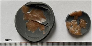
K0.5Na0.5NbO3 (KNN) crystals have great application prospects due to their excellent piezoelectric properties, high Curie temperature, and environmental friendliness. Currently, KNN crystals grown by the seed-free solid-state crystal growth (SFSSCG) method exhibit relatively high dielectric loss. In order to reduce their dielectric loss, Cu, Bi and Mn co-doped KNN lead-free piezoelectric single crystals were prepared by the SFSSCG method. The effects of the CuO doping content on the structure and electrical properties of (1 − x)(0.996KNN–0.004BiMnO3)–xCuO crystals were systematically studied. The results show that an appropriate doping amount of CuO is beneficial for the growth of the crystals and the improvement of electrical properties. When the diameter of the billets is 40 mm, the maximum crystal size of 25 × 21 × 2 mm3 is obtained. All crystals have a typical perovskite structure almost with a single orthorhombic phase and are very compact almost without holes. The minimum average domain width of 276 nm is obtained for the crystal at x = 0.005. The KNN crystals exhibit normal ferroelectric characteristics and a space-charge-limited-conduction (SCLC) mechanism. The introduction of Cu2+ ions reduces the dielectric loss of the crystal and increases its piezoelectric and dielectric properties. The Cu, Bi and Mn co-doped KNN crystals achieve excellent comprehensive properties: d33 = 314 pC N−1, Pr = 29.9 μC cm−2, Ec = 10.1 kV cm−1, = 869 pm V−1, Qm = 56.8, Kt = 0.38, tan δ = 0.013 and TC = 409 °C. This provides a route to improve the electrical properties of KNN-based crystals.
 求助内容:
求助内容: 应助结果提醒方式:


