Anna‐Lena Hofmann, Jakob Wolansky, Mike Hambsch, Felix Talnack, Eva Bittrich, Lucy Winkler, Max Herzog, Tianyi Zhang, Tobias Antrack, L. Conrad Winkler, Jonas Schröder, Moritz Riede, Stefan C.B. Mannsfeld, Johannes Benduhn, Karl Leo
{"title":"应用于有机光电探测器的高有序芘薄膜晶体生长控制策略","authors":"Anna‐Lena Hofmann, Jakob Wolansky, Mike Hambsch, Felix Talnack, Eva Bittrich, Lucy Winkler, Max Herzog, Tianyi Zhang, Tobias Antrack, L. Conrad Winkler, Jonas Schröder, Moritz Riede, Stefan C.B. Mannsfeld, Johannes Benduhn, Karl Leo","doi":"10.1002/adom.202401025","DOIUrl":null,"url":null,"abstract":"Organic semiconductors still lag behind their inorganic counterparts in terms of mobility due to their lower structural order, in particular in thin films. Here, the highly ordered phase of triclinic rubrene – characterized by high vertical hole mobility – grown from a vacuum‐deposited thin film is used by post‐annealing and implemented into organic photodetectors. Since the triclinic rubrene exhibits a high roughness with a peak‐to‐valley value of 250 nm, which is detrimental to the dark current, strategies to control the crystal growth are developed. These investigations show that a suppression layer of 20 nm C<jats:sub>60</jats:sub> is the most promising approach to successfully reduce the surface roughness while maintaining the triclinic phase, proven by grazing‐incidence wide‐angle X‐ray scattering (GIWAXS). With the smoothened active layer, the dark current density is reduced by three orders of magnitude compared to the neat rubrene layer. It is as low as 2.5 × 10<jats:sup>−10 </jats:sup>A cm<jats:sup>−2</jats:sup> at −0.1 V bias, reflected in an overall specific detectivity of 6 × 10<jats:sup>11</jats:sup> Jones at zero bias (based on noise measurements) and a high linear dynamic range of 170 dB. This strategy using a suppression layer thus proves successful and is very promising to be applied to other crystalline materials.","PeriodicalId":116,"journal":{"name":"Advanced Optical Materials","volume":null,"pages":null},"PeriodicalIF":8.0000,"publicationDate":"2024-06-29","publicationTypes":"Journal Article","fieldsOfStudy":null,"isOpenAccess":false,"openAccessPdf":"","citationCount":"0","resultStr":"{\"title\":\"Strategies to Control Crystal Growth of Highly Ordered Rubrene Thin Films for Application in Organic Photodetectors\",\"authors\":\"Anna‐Lena Hofmann, Jakob Wolansky, Mike Hambsch, Felix Talnack, Eva Bittrich, Lucy Winkler, Max Herzog, Tianyi Zhang, Tobias Antrack, L. Conrad Winkler, Jonas Schröder, Moritz Riede, Stefan C.B. Mannsfeld, Johannes Benduhn, Karl Leo\",\"doi\":\"10.1002/adom.202401025\",\"DOIUrl\":null,\"url\":null,\"abstract\":\"Organic semiconductors still lag behind their inorganic counterparts in terms of mobility due to their lower structural order, in particular in thin films. Here, the highly ordered phase of triclinic rubrene – characterized by high vertical hole mobility – grown from a vacuum‐deposited thin film is used by post‐annealing and implemented into organic photodetectors. Since the triclinic rubrene exhibits a high roughness with a peak‐to‐valley value of 250 nm, which is detrimental to the dark current, strategies to control the crystal growth are developed. These investigations show that a suppression layer of 20 nm C<jats:sub>60</jats:sub> is the most promising approach to successfully reduce the surface roughness while maintaining the triclinic phase, proven by grazing‐incidence wide‐angle X‐ray scattering (GIWAXS). With the smoothened active layer, the dark current density is reduced by three orders of magnitude compared to the neat rubrene layer. It is as low as 2.5 × 10<jats:sup>−10 </jats:sup>A cm<jats:sup>−2</jats:sup> at −0.1 V bias, reflected in an overall specific detectivity of 6 × 10<jats:sup>11</jats:sup> Jones at zero bias (based on noise measurements) and a high linear dynamic range of 170 dB. This strategy using a suppression layer thus proves successful and is very promising to be applied to other crystalline materials.\",\"PeriodicalId\":116,\"journal\":{\"name\":\"Advanced Optical Materials\",\"volume\":null,\"pages\":null},\"PeriodicalIF\":8.0000,\"publicationDate\":\"2024-06-29\",\"publicationTypes\":\"Journal Article\",\"fieldsOfStudy\":null,\"isOpenAccess\":false,\"openAccessPdf\":\"\",\"citationCount\":\"0\",\"resultStr\":null,\"platform\":\"Semanticscholar\",\"paperid\":null,\"PeriodicalName\":\"Advanced Optical Materials\",\"FirstCategoryId\":\"88\",\"ListUrlMain\":\"https://doi.org/10.1002/adom.202401025\",\"RegionNum\":2,\"RegionCategory\":\"材料科学\",\"ArticlePicture\":[],\"TitleCN\":null,\"AbstractTextCN\":null,\"PMCID\":null,\"EPubDate\":\"\",\"PubModel\":\"\",\"JCR\":\"Q1\",\"JCRName\":\"MATERIALS SCIENCE, MULTIDISCIPLINARY\",\"Score\":null,\"Total\":0}","platform":"Semanticscholar","paperid":null,"PeriodicalName":"Advanced Optical Materials","FirstCategoryId":"88","ListUrlMain":"https://doi.org/10.1002/adom.202401025","RegionNum":2,"RegionCategory":"材料科学","ArticlePicture":[],"TitleCN":null,"AbstractTextCN":null,"PMCID":null,"EPubDate":"","PubModel":"","JCR":"Q1","JCRName":"MATERIALS SCIENCE, MULTIDISCIPLINARY","Score":null,"Total":0}
引用次数: 0
摘要
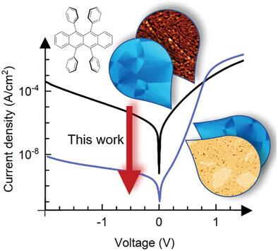
由于结构有序性较低,有机半导体在迁移率方面仍然落后于无机半导体,尤其是在薄膜中。在这里,利用真空沉积薄膜生长出的高度有序的三菱红柱石相(具有高垂直空穴迁移率的特点)进行后退火,并将其应用到有机光电探测器中。由于三linic rubrene 具有峰谷值为 250 nm 的高粗糙度,不利于暗电流,因此开发了控制晶体生长的策略。通过掠入射广角 X 射线散射 (GIWAXS),这些研究表明 20 nm C60 抑制层是在保持三菱相的同时成功降低表面粗糙度的最有前途的方法。与纯红宝石层相比,平滑活性层的暗电流密度降低了三个数量级。在 -0.1 V 偏压下,暗电流密度低至 2.5 × 10⁻¹⁰ A cm-2,这反映在零偏压下 6 × 10¹¹ Jones 的总体特定检测率(基于噪声测量)和 170 dB 的高线性动态范围上。因此,这种使用抑制层的策略被证明是成功的,并有望应用于其他晶体材料。
Strategies to Control Crystal Growth of Highly Ordered Rubrene Thin Films for Application in Organic Photodetectors
Organic semiconductors still lag behind their inorganic counterparts in terms of mobility due to their lower structural order, in particular in thin films. Here, the highly ordered phase of triclinic rubrene – characterized by high vertical hole mobility – grown from a vacuum‐deposited thin film is used by post‐annealing and implemented into organic photodetectors. Since the triclinic rubrene exhibits a high roughness with a peak‐to‐valley value of 250 nm, which is detrimental to the dark current, strategies to control the crystal growth are developed. These investigations show that a suppression layer of 20 nm C60 is the most promising approach to successfully reduce the surface roughness while maintaining the triclinic phase, proven by grazing‐incidence wide‐angle X‐ray scattering (GIWAXS). With the smoothened active layer, the dark current density is reduced by three orders of magnitude compared to the neat rubrene layer. It is as low as 2.5 × 10⁻¹⁰ A cm−2 at −0.1 V bias, reflected in an overall specific detectivity of 6 × 10¹¹ Jones at zero bias (based on noise measurements) and a high linear dynamic range of 170 dB. This strategy using a suppression layer thus proves successful and is very promising to be applied to other crystalline materials.
期刊介绍:
Advanced Optical Materials, part of the esteemed Advanced portfolio, is a unique materials science journal concentrating on all facets of light-matter interactions. For over a decade, it has been the preferred optical materials journal for significant discoveries in photonics, plasmonics, metamaterials, and more. The Advanced portfolio from Wiley is a collection of globally respected, high-impact journals that disseminate the best science from established and emerging researchers, aiding them in fulfilling their mission and amplifying the reach of their scientific discoveries.