通过卤化物气相外延生长厚ε(κ)-Ga2O3 薄膜

IF 0.8 4区 物理与天体物理 Q4 PHYSICS, APPLIED
S. I. Stepanov, A. I. Pechnikov, M. P. Scheglov, A. V. Chikiryaka, V. I. Nikolaev
{"title":"通过卤化物气相外延生长厚ε(κ)-Ga2O3 薄膜","authors":"S. I. Stepanov, A. I. Pechnikov, M. P. Scheglov, A. V. Chikiryaka, V. I. Nikolaev","doi":"10.1134/s1063785023900583","DOIUrl":null,"url":null,"abstract":"<h3 data-test=\"abstract-sub-heading\">\n<b>Abstract</b>\n</h3><p>High crystalline quality epitaxial films of orthorhombic gallium oxide ε(κ)-Ga<sub>2</sub>O<sub>3</sub> with a thickness of more 20 μm have been grown for the first time using halide vapor phase epitaxy. Sapphire wafers with preliminarily deposited GaN layers were used as substrates. The properties of the produced films are studied by X-ray diffraction and electron microscopy. The results are considered an important step towards obtaining thick layers and quasi-bulk ε<b>(</b>κ)-Ga<sub>2</sub>O<sub>3</sub> crystals for practical applications in electronics and sensor technology.</p>","PeriodicalId":784,"journal":{"name":"Technical Physics Letters","volume":null,"pages":null},"PeriodicalIF":0.8000,"publicationDate":"2024-03-14","publicationTypes":"Journal Article","fieldsOfStudy":null,"isOpenAccess":false,"openAccessPdf":"","citationCount":"0","resultStr":"{\"title\":\"Growth of Thick ε(κ)-Ga2O3 Films by Halide Vapor Phase Epitaxy\",\"authors\":\"S. I. Stepanov, A. I. Pechnikov, M. P. Scheglov, A. V. Chikiryaka, V. I. Nikolaev\",\"doi\":\"10.1134/s1063785023900583\",\"DOIUrl\":null,\"url\":null,\"abstract\":\"<h3 data-test=\\\"abstract-sub-heading\\\">\\n<b>Abstract</b>\\n</h3><p>High crystalline quality epitaxial films of orthorhombic gallium oxide ε(κ)-Ga<sub>2</sub>O<sub>3</sub> with a thickness of more 20 μm have been grown for the first time using halide vapor phase epitaxy. Sapphire wafers with preliminarily deposited GaN layers were used as substrates. The properties of the produced films are studied by X-ray diffraction and electron microscopy. The results are considered an important step towards obtaining thick layers and quasi-bulk ε<b>(</b>κ)-Ga<sub>2</sub>O<sub>3</sub> crystals for practical applications in electronics and sensor technology.</p>\",\"PeriodicalId\":784,\"journal\":{\"name\":\"Technical Physics Letters\",\"volume\":null,\"pages\":null},\"PeriodicalIF\":0.8000,\"publicationDate\":\"2024-03-14\",\"publicationTypes\":\"Journal Article\",\"fieldsOfStudy\":null,\"isOpenAccess\":false,\"openAccessPdf\":\"\",\"citationCount\":\"0\",\"resultStr\":null,\"platform\":\"Semanticscholar\",\"paperid\":null,\"PeriodicalName\":\"Technical Physics Letters\",\"FirstCategoryId\":\"101\",\"ListUrlMain\":\"https://doi.org/10.1134/s1063785023900583\",\"RegionNum\":4,\"RegionCategory\":\"物理与天体物理\",\"ArticlePicture\":[],\"TitleCN\":null,\"AbstractTextCN\":null,\"PMCID\":null,\"EPubDate\":\"\",\"PubModel\":\"\",\"JCR\":\"Q4\",\"JCRName\":\"PHYSICS, APPLIED\",\"Score\":null,\"Total\":0}","platform":"Semanticscholar","paperid":null,"PeriodicalName":"Technical Physics Letters","FirstCategoryId":"101","ListUrlMain":"https://doi.org/10.1134/s1063785023900583","RegionNum":4,"RegionCategory":"物理与天体物理","ArticlePicture":[],"TitleCN":null,"AbstractTextCN":null,"PMCID":null,"EPubDate":"","PubModel":"","JCR":"Q4","JCRName":"PHYSICS, APPLIED","Score":null,"Total":0}
引用次数: 0

摘要

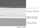
摘要 利用卤化物气相外延技术首次生长出厚度超过 20 μm 的正交氧化镓ε(κ)-Ga2O3 高结晶质量外延薄膜。基片使用了初步沉积了 GaN 层的蓝宝石晶片。通过 X 射线衍射和电子显微镜研究了所制备薄膜的特性。这些结果被认为是获得厚层和准大体积ε(κ)-Ga2O3晶体的重要一步,可用于电子和传感器技术的实际应用。
本文章由计算机程序翻译,如有差异,请以英文原文为准。

Growth of Thick ε(κ)-Ga2O3 Films by Halide Vapor Phase Epitaxy

Growth of Thick ε(κ)-Ga2O3 Films by Halide Vapor Phase Epitaxy

Abstract

High crystalline quality epitaxial films of orthorhombic gallium oxide ε(κ)-Ga2O3 with a thickness of more 20 μm have been grown for the first time using halide vapor phase epitaxy. Sapphire wafers with preliminarily deposited GaN layers were used as substrates. The properties of the produced films are studied by X-ray diffraction and electron microscopy. The results are considered an important step towards obtaining thick layers and quasi-bulk ε(κ)-Ga2O3 crystals for practical applications in electronics and sensor technology.

求助全文
通过发布文献求助,成功后即可免费获取论文全文。 去求助
来源期刊
Technical Physics Letters
Technical Physics Letters 物理-物理:应用
CiteScore
1.50
自引率
0.00%
发文量
44
审稿时长
2-4 weeks
期刊介绍: Technical Physics Letters is a companion journal to Technical Physics and offers rapid publication of developments in theoretical and experimental physics with potential technological applications. Recent emphasis has included many papers on gas lasers and on lasing in semiconductors, as well as many reports on high Tc superconductivity. The excellent coverage of plasma physics seen in the parent journal, Technical Physics, is also present here with quick communication of developments in theoretical and experimental work in all fields with probable technical applications. Topics covered are basic and applied physics; plasma physics; solid state physics; physical electronics; accelerators; microwave electron devices; holography.
×
引用
GB/T 7714-2015
复制
MLA
复制
APA
复制
导出至
BibTeX EndNote RefMan NoteFirst NoteExpress
×
提示
您的信息不完整,为了账户安全,请先补充。
现在去补充
×
提示
您因"违规操作"
具体请查看互助需知
我知道了
×
提示
确定
请完成安全验证×
copy
已复制链接
快去分享给好友吧!
我知道了
右上角分享
点击右上角分享
0
联系我们:info@booksci.cn Book学术提供免费学术资源搜索服务,方便国内外学者检索中英文文献。致力于提供最便捷和优质的服务体验。 Copyright © 2023 布克学术 All rights reserved.
京ICP备2023020795号-1
ghs 京公网安备 11010802042870号
Book学术文献互助
Book学术文献互助群
群 号:481959085
Book学术官方微信