{"title":"
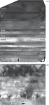
应力 InAs/GaSb 超晶格中的层生长特征","authors":"R. V. Levin, V. N. Nevedomskiy, L. A. Sokura","doi":"10.1134/s1063785023900376","DOIUrl":null,"url":null,"abstract":"<h3 data-test=\"abstract-sub-heading\">Abstract</h3><p>The paper presents the results of a study of factors affecting the thickness of transition (interface) layers in stressed InAs/GaSb superlattices during growth by MOCVD method. It is shown that the thicknesses of the interface layers between InAs and GaSb are practically independent of the growth temperature. The thickness of the interface layers is influenced by the direction of switching the layer growth. The smallest thickness of 1.2–1.4 nm of the interface layer InAs/GaSb was obtained for the direction of growth switching from GaSb to InAs.</p>","PeriodicalId":784,"journal":{"name":"Technical Physics Letters","volume":null,"pages":null},"PeriodicalIF":0.8000,"publicationDate":"2024-03-13","publicationTypes":"Journal Article","fieldsOfStudy":null,"isOpenAccess":false,"openAccessPdf":"","citationCount":"0","resultStr":"{\"title\":\"The Features of the Layers Growth in Stressed InAs/GaSb Superlattices\",\"authors\":\"R. V. Levin, V. N. Nevedomskiy, L. A. Sokura\",\"doi\":\"10.1134/s1063785023900376\",\"DOIUrl\":null,\"url\":null,\"abstract\":\"<h3 data-test=\\\"abstract-sub-heading\\\">Abstract</h3><p>The paper presents the results of a study of factors affecting the thickness of transition (interface) layers in stressed InAs/GaSb superlattices during growth by MOCVD method. It is shown that the thicknesses of the interface layers between InAs and GaSb are practically independent of the growth temperature. The thickness of the interface layers is influenced by the direction of switching the layer growth. The smallest thickness of 1.2–1.4 nm of the interface layer InAs/GaSb was obtained for the direction of growth switching from GaSb to InAs.</p>\",\"PeriodicalId\":784,\"journal\":{\"name\":\"Technical Physics Letters\",\"volume\":null,\"pages\":null},\"PeriodicalIF\":0.8000,\"publicationDate\":\"2024-03-13\",\"publicationTypes\":\"Journal Article\",\"fieldsOfStudy\":null,\"isOpenAccess\":false,\"openAccessPdf\":\"\",\"citationCount\":\"0\",\"resultStr\":null,\"platform\":\"Semanticscholar\",\"paperid\":null,\"PeriodicalName\":\"Technical Physics Letters\",\"FirstCategoryId\":\"101\",\"ListUrlMain\":\"https://doi.org/10.1134/s1063785023900376\",\"RegionNum\":4,\"RegionCategory\":\"物理与天体物理\",\"ArticlePicture\":[],\"TitleCN\":null,\"AbstractTextCN\":null,\"PMCID\":null,\"EPubDate\":\"\",\"PubModel\":\"\",\"JCR\":\"Q4\",\"JCRName\":\"PHYSICS, APPLIED\",\"Score\":null,\"Total\":0}","platform":"Semanticscholar","paperid":null,"PeriodicalName":"Technical Physics Letters","FirstCategoryId":"101","ListUrlMain":"https://doi.org/10.1134/s1063785023900376","RegionNum":4,"RegionCategory":"物理与天体物理","ArticlePicture":[],"TitleCN":null,"AbstractTextCN":null,"PMCID":null,"EPubDate":"","PubModel":"","JCR":"Q4","JCRName":"PHYSICS, APPLIED","Score":null,"Total":0}
The Features of the Layers Growth in Stressed InAs/GaSb Superlattices
Abstract
The paper presents the results of a study of factors affecting the thickness of transition (interface) layers in stressed InAs/GaSb superlattices during growth by MOCVD method. It is shown that the thicknesses of the interface layers between InAs and GaSb are practically independent of the growth temperature. The thickness of the interface layers is influenced by the direction of switching the layer growth. The smallest thickness of 1.2–1.4 nm of the interface layer InAs/GaSb was obtained for the direction of growth switching from GaSb to InAs.
期刊介绍:
Technical Physics Letters is a companion journal to Technical Physics and offers rapid publication of developments in theoretical and experimental physics with potential technological applications. Recent emphasis has included many papers on gas lasers and on lasing in semiconductors, as well as many reports on high Tc superconductivity. The excellent coverage of plasma physics seen in the parent journal, Technical Physics, is also present here with quick communication of developments in theoretical and experimental work in all fields with probable technical applications. Topics covered are basic and applied physics; plasma physics; solid state physics; physical electronics; accelerators; microwave electron devices; holography.