Di Wu, Chenguang Guo, Longhui Zeng, Xiaoyan Ren, Zhifeng Shi, Long Wen, Qin Chen, Meng Zhang, Xin Jian Li, Chong-Xin Shan, Jiansheng Jie
{"title":"Phase-controlled van der Waals growth of wafer-scale 2D MoTe<sub>2</sub> layers for integrated high-sensitivity broadband infrared photodetection.","authors":"Di Wu, Chenguang Guo, Longhui Zeng, Xiaoyan Ren, Zhifeng Shi, Long Wen, Qin Chen, Meng Zhang, Xin Jian Li, Chong-Xin Shan, Jiansheng Jie","doi":"10.1038/s41377-022-01047-5","DOIUrl":null,"url":null,"abstract":"<p><p>Being capable of sensing broadband infrared (IR) light is vitally important for wide-ranging applications from fundamental science to industrial purposes. Two-dimensional (2D) topological semimetals are being extensively explored for broadband IR detection due to their gapless electronic structure and the linear energy dispersion relation. However, the low charge separation efficiency, high noise level, and on-chip integration difficulty of these semimetals significantly hinder their further technological applications. Here, we demonstrate a facile thermal-assisted tellurization route for the van der Waals (vdW) growth of wafer-scale phase-controlled 2D MoTe<sub>2</sub> layers. Importantly, the type-II Weyl semimetal 1T'-MoTe<sub>2</sub> features a unique orthorhombic lattice structure with a broken inversion symmetry, which ensures efficient carrier transportation and thus reduces the carrier recombination. This characteristic is a key merit for the well-designed 1T'-MoTe<sub>2</sub>/Si vertical Schottky junction photodetector to achieve excellent performance with an ultrabroadband detection range of up to 10.6 µm and a large room temperature specific detectivity of over 10<sup>8</sup> Jones in the mid-infrared (MIR) range. Moreover, the large-area synthesis of 2D MoTe<sub>2</sub> layers enables the demonstration of high-resolution uncooled MIR imaging capability by using an integrated device array. This work provides a new approach to assembling uncooled IR photodetectors based on 2D materials.</p>","PeriodicalId":18093,"journal":{"name":"Light, science & applications","volume":"12 1","pages":"5"},"PeriodicalIF":19.4000,"publicationDate":"2023-01-02","publicationTypes":"Journal Article","fieldsOfStudy":null,"isOpenAccess":false,"openAccessPdf":"https://www.ncbi.nlm.nih.gov/pmc/articles/PMC9806107/pdf/","citationCount":"38","resultStr":null,"platform":"Semanticscholar","paperid":null,"PeriodicalName":"Light, science & applications","FirstCategoryId":"101","ListUrlMain":"https://doi.org/10.1038/s41377-022-01047-5","RegionNum":1,"RegionCategory":"物理与天体物理","ArticlePicture":[],"TitleCN":null,"AbstractTextCN":null,"PMCID":null,"EPubDate":"","PubModel":"","JCR":"Q1","JCRName":"Physics and Astronomy","Score":null,"Total":0}
引用次数: 38
Abstract
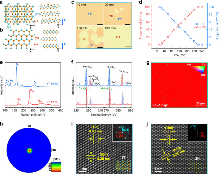
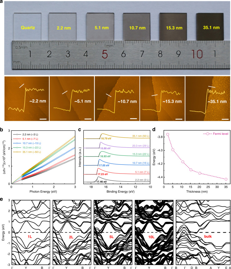
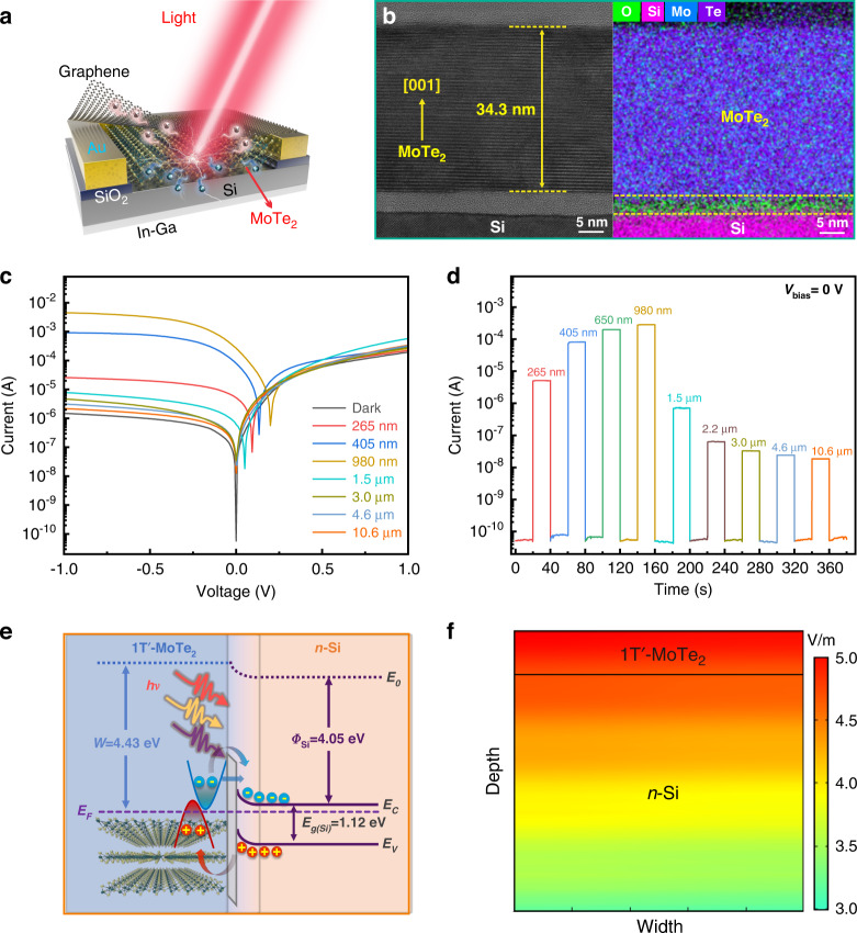
Being capable of sensing broadband infrared (IR) light is vitally important for wide-ranging applications from fundamental science to industrial purposes. Two-dimensional (2D) topological semimetals are being extensively explored for broadband IR detection due to their gapless electronic structure and the linear energy dispersion relation. However, the low charge separation efficiency, high noise level, and on-chip integration difficulty of these semimetals significantly hinder their further technological applications. Here, we demonstrate a facile thermal-assisted tellurization route for the van der Waals (vdW) growth of wafer-scale phase-controlled 2D MoTe2 layers. Importantly, the type-II Weyl semimetal 1T'-MoTe2 features a unique orthorhombic lattice structure with a broken inversion symmetry, which ensures efficient carrier transportation and thus reduces the carrier recombination. This characteristic is a key merit for the well-designed 1T'-MoTe2/Si vertical Schottky junction photodetector to achieve excellent performance with an ultrabroadband detection range of up to 10.6 µm and a large room temperature specific detectivity of over 108 Jones in the mid-infrared (MIR) range. Moreover, the large-area synthesis of 2D MoTe2 layers enables the demonstration of high-resolution uncooled MIR imaging capability by using an integrated device array. This work provides a new approach to assembling uncooled IR photodetectors based on 2D materials.
期刊介绍:
Light: Science & Applications is an open-access, fully peer-reviewed publication.It publishes high-quality optics and photonics research globally, covering fundamental research and important issues in engineering and applied sciences related to optics and photonics.
 求助内容:
求助内容: 应助结果提醒方式:


