{"title":"Optimized process for fabrication of free-standing silicon nanophotonic devices.","authors":"Paul Seidler","doi":"10.1116/1.4983173","DOIUrl":null,"url":null,"abstract":"<p><p>A detailed procedure is presented for fabrication of free-standing silicon photonic devices that accurately reproduces design dimensions while minimizing surface roughness. By reducing charging effects during inductively coupled-plasma reactive ion etching, undercutting in small, high-aspect ratio openings is reduced. Slot structures with a width as small as 40 nm and an aspect ratio of 5.5:1 can be produced with a nearly straight, vertical sidewall profile. Subsequent removal of an underlying sacrificial silicon dioxide layer by wet-etching to create free-standing devices is performed under conditions which suppress attack of the silicon. Slotted one-dimensional photonic crystal cavities are used as sensitive test structures to demonstrate that performance specifications can be reached without iteratively adapting design dimensions; optical resonance frequencies are within 1% of the simulated values and quality factors on the order of 10<sup>5</sup> are routinely attained.</p>","PeriodicalId":74007,"journal":{"name":"","volume":"35 3","pages":"031209"},"PeriodicalIF":0.0,"publicationDate":"2017-05-01","publicationTypes":"Journal Article","fieldsOfStudy":null,"isOpenAccess":false,"openAccessPdf":"https://www.ncbi.nlm.nih.gov/pmc/articles/PMC5429187/pdf/","citationCount":"0","resultStr":null,"platform":"Semanticscholar","paperid":null,"PeriodicalName":"","FirstCategoryId":"5","ListUrlMain":"https://doi.org/10.1116/1.4983173","RegionNum":0,"RegionCategory":null,"ArticlePicture":[],"TitleCN":null,"AbstractTextCN":null,"PMCID":null,"EPubDate":"2017/5/12 0:00:00","PubModel":"Epub","JCR":"","JCRName":"","Score":null,"Total":0}
引用次数: 0
Abstract
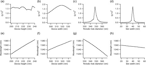
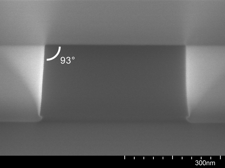
A detailed procedure is presented for fabrication of free-standing silicon photonic devices that accurately reproduces design dimensions while minimizing surface roughness. By reducing charging effects during inductively coupled-plasma reactive ion etching, undercutting in small, high-aspect ratio openings is reduced. Slot structures with a width as small as 40 nm and an aspect ratio of 5.5:1 can be produced with a nearly straight, vertical sidewall profile. Subsequent removal of an underlying sacrificial silicon dioxide layer by wet-etching to create free-standing devices is performed under conditions which suppress attack of the silicon. Slotted one-dimensional photonic crystal cavities are used as sensitive test structures to demonstrate that performance specifications can be reached without iteratively adapting design dimensions; optical resonance frequencies are within 1% of the simulated values and quality factors on the order of 105 are routinely attained.
 求助内容:
求助内容: 应助结果提醒方式:


