{"title":"Distinct Design for Two Terminal Crystalline Silicon Bottom-Based III–V Tandem Devices via Direct Electrode Interconnection and Enlarged Bottom Area","authors":"Muhammad Aleem Zahid, , , Seungyong Han, , , Syed Azkar UI Hasan, , , Vinh-Ai Dao, , , Minh Phuong Nguyen, , , Duy Phong Pham*, , and , Junsin Yi*, ","doi":"10.1021/acsaem.5c01220","DOIUrl":null,"url":null,"abstract":"<p >An innovative two-terminal III–V/c-Si multijunction device is constructed using direct electrode connections and extending the bottom area to improve carrier transport and current matching between the top III–V and bottom c-Si devices. A commercial triple junction GaInP<sub>2</sub>/InGaAs/Ge top cell (1 cm<sup>2</sup>) with a complete cover electrode at the rear is connected directly to a silicon heterojunction (SHJ) bottom device using silver paste. The area of the SHJ bottom device is enlarged from 0.69 cm<sup>2</sup> to 15 cm<sup>2</sup> to match the current density of the top. With a small active area of 0.69 cm<sup>2</sup>, the bottom device has a current density of 13.6 mA/cm<sup>2</sup>, comparable to the top device’s (13.5 mA/cm<sup>2</sup>). By optimizing the SHJ bottom, the multijunction device achieves an impressive efficiency of 39.5% with a short circuit current density of 13.5 mA/cm<sup>2</sup>, an open circuit voltage of 3.45 V, and an 85% fill factor. This initial design demonstrates the potential to significantly improve the efficiency of a two-terminal III–V/c-Si tandem device by increasing the matching current levels of both top and bottom cells.</p>","PeriodicalId":4,"journal":{"name":"ACS Applied Energy Materials","volume":"8 19","pages":"14086–14092"},"PeriodicalIF":5.5000,"publicationDate":"2025-09-21","publicationTypes":"Journal Article","fieldsOfStudy":null,"isOpenAccess":false,"openAccessPdf":"","citationCount":"0","resultStr":null,"platform":"Semanticscholar","paperid":null,"PeriodicalName":"ACS Applied Energy Materials","FirstCategoryId":"88","ListUrlMain":"https://pubs.acs.org/doi/10.1021/acsaem.5c01220","RegionNum":3,"RegionCategory":"材料科学","ArticlePicture":[],"TitleCN":null,"AbstractTextCN":null,"PMCID":null,"EPubDate":"","PubModel":"","JCR":"Q2","JCRName":"CHEMISTRY, PHYSICAL","Score":null,"Total":0}
引用次数: 0
Abstract
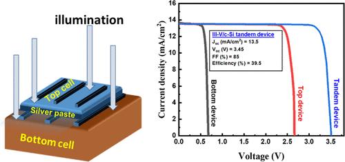
An innovative two-terminal III–V/c-Si multijunction device is constructed using direct electrode connections and extending the bottom area to improve carrier transport and current matching between the top III–V and bottom c-Si devices. A commercial triple junction GaInP2/InGaAs/Ge top cell (1 cm2) with a complete cover electrode at the rear is connected directly to a silicon heterojunction (SHJ) bottom device using silver paste. The area of the SHJ bottom device is enlarged from 0.69 cm2 to 15 cm2 to match the current density of the top. With a small active area of 0.69 cm2, the bottom device has a current density of 13.6 mA/cm2, comparable to the top device’s (13.5 mA/cm2). By optimizing the SHJ bottom, the multijunction device achieves an impressive efficiency of 39.5% with a short circuit current density of 13.5 mA/cm2, an open circuit voltage of 3.45 V, and an 85% fill factor. This initial design demonstrates the potential to significantly improve the efficiency of a two-terminal III–V/c-Si tandem device by increasing the matching current levels of both top and bottom cells.
期刊介绍:
ACS Applied Energy Materials is an interdisciplinary journal publishing original research covering all aspects of materials, engineering, chemistry, physics and biology relevant to energy conversion and storage. The journal is devoted to reports of new and original experimental and theoretical research of an applied nature that integrate knowledge in the areas of materials, engineering, physics, bioscience, and chemistry into important energy applications.
 求助内容:
求助内容: 应助结果提醒方式:


